3 - 31
GRUNDIG Service
Schaltpläne und Platinenabbildungen / Circuit Diagrams and Layout of PCBs
M 49-DPL
IC703, IC704 LB1641
IC202 STK400-090
IC203 UPC1237HA
IC702 LA6537
Page 1: ...9 4000 nderungen vorbehalten Subject to alteration Printed in Germany W E BS 38 0599 8002 8012 8005 8015 8006 8016 http www grundig de M 49 DPL G LI 0751 Grundig Service Hotline Deutschland TV TV SAT...
Page 2: ...9 Adjustment Procedures 2 3 2 5 Circuit Diagrams and Layout of the PCBs 3 1 3 36 Block Diagram 3 1 Wiring Diagram 3 2 Circuit Diagrams Mains Unit Board 3 4 CD Key Board Control Board 3 10 Headphone Bo...
Page 3: ...dB Gleichlaufschwankungen 0 25 GEH USE Material Oberfl che Polystyrol und Metall Abmessungen B x H x T 280 x 310 x 360mm Gewicht mit Lautsprechern ca 12 19kg Technical Data AMPLIFIER Output power Musi...
Page 4: ...bedienung Die gew hlte Signalquelle l uft einmal ber das Display Hinweis Bei der Wahl der AUX Signalquelle ist sicher zustellen da der linke und der rechte Ausgang des externen Ger tes z B TV oder VCR...
Page 5: ...Der Sender und die Speicherplatznummer werden gespeichert und die Angabe STORED wird angezeigt Die obigen Schritte wiederholen um weitere Vorwahlsender zu speichern Hinweis Bei einer Unterbrechung de...
Page 6: ...hritten 4 bis 9 fort 4 Dr cken Sie die Taste TIMER um die Wahl der Signalquelle zu best tigen Die Angabe START wird angezeigt Auf dem Display erscheint 0O 00 und 00 blinkt 5 Dr cken Sie die Taste A od...
Page 7: ...et is in Normal Stereo mode When you have completed the Dolby Pro Logic setup you are ready to experience and enjoy a Home Cinema sound ambience Press DOLBY SURROUND on the unit or SURR MODE on the re...
Page 8: ...ld RECORD on the unit or on the remote control for 1 second CD SYNCHRO scrolls across the display The RECORD flag appears on the display The CD starts playing after a seven second delay to prevent rec...
Page 9: ...kt 2 5 Schrauben I Fig 3 und Schraube J Fig 4 herausschrauben Hauptplatte herausnehmen dabei Steckverbinder nach Bedarf ff nen Disassembly Instructions 1 Opening the Cabinet Undo 6 screws on each side...
Page 10: ...Schrauben T herausschrauben und die Steuerplatte V abneh men 3 Schrauben U sind f r die Befestigung der Tastenst el 5 Removing the Cassette Compartment Lid Fig 6 Open the cassette compartment press in...
Page 11: ...e ausbauen Pkt 9 5 Schrauben K Fig 5 herausschrauben 4 Schrauben C Fig 8 herausschrauben Trafo F Fig 10 mit Tr gerplatte herausnehmen 4 Schrauben D Fig 10 herausschrauben und Tr gerplatte abneh men 7...
Page 12: ...n Beim Herausziehen der Flexprint Leitung die se dann nach unten ber die Kontakte schieben MOS Bauteile 16 Drehtellerantrieb ausbauen Die 3 Schrauben G Fig 11 herausschrauben und das Blech H abnehmen...
Page 13: ...usbauen Cassettenlaufwerk ausbauen Pkt 17 Rastnase c ausrasten und Andruckrollenhebel nach oben abzie hen Fig 18 17 Removing the Cassette Drive Mechanism Remove the Front para 3 Undo 4 screws b and re...
Page 14: ...en Fig 21 22 Drehkopf ausbauen Cassettenlaufwerk ausbauen Pkt 17 Tonkopfleitungen abl ten 2 Schrauben k herausschrauben und den Tonkopf entnehmen Fig 22 19 Removing the Cassette Drive Motor Remove the...
Page 15: ...n Ua nur so gro da das Signal gerade erkennbar ist m 30 fmod 1kHz NF VoltmeteroderOszilloskopanLautsprecheranschlu MW Me sendersignal an Antennenklemmen einspeisen Ua nur so gro da das Signal gerade e...
Page 16: ...n Aufnahme wiederholen und pr fen Mit T602 und T603 auf Minimum einstellen Mit T601 auf 100kHz 1kHz einstellen normal reverse Die Einstellschrauben der Tonk pfe sind durch kleine Aussparungen in der F...
Page 17: ...tend ZF Filter IF Filter FM AM AUX IN SUBWOOFER OUT L R CENTER L SURROUND R Pin 8 Pin 9 Abgleichelemente Tuner Alignment Elements Tuner 1 9 1 18 19 36 1 1 TP1 Deck A Deck B Deck A Deck B Deck B Deck A...
Page 18: ...IC301 Pin 9 MW DC voltmeter to Frontend Pin 5 VT LW DC voltmeter to Frontend Pin 5 VT MW Sweep generator 450kHz to aerial inputs Uout as low as possible m 30 fmod 1kHz AF voltmeter or oscilloscope to...
Page 19: ...d again and check With T602 and T603 adjust for Minimum With T601 adjust for 100kHz 1kHz Access to the adjustment screws of the audio heads is possible through small cutouts on the front panel If ther...
Page 20: ...1 GRUNDIG Service Schaltpl ne und Platinenabbildungen Circuit Diagrams and Layout of PCBs M 49 DPL Schaltpl ne und Platinenabbildungen Circuit Diagrams and Layout of PCBs Blockschaltplan Block Diagra...
Page 21: ...MOTOR ROT MOTOR AD SW ST SW TUDN TUUP SW S709 TRAFO TAPE A CRH4428 TAPE B CRH4427 HAUPTPLATTE MAIN BOARD CD PLATTE CD BOARD CD LAUFWERK CD DRIVE MECHANISM NETZTEILPLATTE MAINS UNIT BOARD VERST RKERPL...
Page 22: ...ldungen Circuit Diagrams and Layout of PCBs M 49 DPL M 49 DPL TO S203 AMPLIFIER BOARD PAGE 3 20 H101 H102 TO H305 MAIN BOARD PAGE 3 12 TO S204 AMPLIFIER BOARD PAGE 3 20 S102 TO H501 CONTROL BOARD PAGE...
Page 23: ...S9 S10 S11 S12 S13 S14 S15 S16 G7 S1 S2 S3 S4 S5 PRESET S7 S8 S9 S10 S11 S12 S13 S14 S15 G8 S1 S2 S3 S4 S5 STEREO S7 S8 S9 S10 S11 S12 S13 S14 S15 TUNED G9 S1 S2 S3 S4 S5 S6 S7 S8 S9 S10 S11 S12 S13 S...
Page 24: ...86 0V PIN 19 4 8V PIN 53 12V PIN 87 0V PIN 20 4 8V PIN 54 13V PIN 88 0V PIN 21 4 8V PIN 55 12V PIN 89 0V PIN 22 0V PIN 56 5V PIN 90 0V PIN 23 4 7V PIN 57 16V PIN 91 4 7V PIN 24 4 7V PIN 58 16V PIN 92...
Page 25: ...2 3 4 5 6 7 8 9 10 11 12 13 14 15 16 1 2 3 4 5 6 7 8 9 10 11 12 13 14 15 16 17 18 R548 10K R549 10K R546 10K 10K 5V R547 W R Q R588 2 2K R586 R585 2 2K DISC1 DISC2 DISC3 SW525 SW526 SW527 5V R519 10K...
Page 26: ...26 27 R BPF2 OSC L BPF3 49 50 51 52 53 64 63 62 61 60 59 58 57 56 55 54 32 LFOUT LRIN LRCOM LROUT LVREF VSS CE DI CL VREF RVREF AROUT ARCOM LINVIN1 L5 L4 L3 L2 L1 VDD R1 R2 RR3 R4 R5 RINVIN RSELO RTI...
Page 27: ...4 1V PIN 39 4 2V PIN 8 4 3V PIN 40 4 4V PIN 9 4 2V PIN 41 4 1V PIN10 4 1V PIN 42 4 2V PIN 11 4 3V PIN 43 4 4V PIN 12 4 2V PIN 44 4 1V PIN 13 4 1V PIN 45 4 2V PIN 14 4 1V PIN 46 4 3V PIN 15 4 3V PIN 47...
Page 28: ...o E B C Q300 0V 0V 0V DTC343 Q301 0V 0 6V 0V 2SC3330 Q302 0V 0 7V 0V 2SC3330 Q303 0V 0V 0V DTC343 Q304 0V 0 7V 0V 2SC3330 Q305 0 8V 1 5V 11V 2SC2999 Q306 12 1V 11V 12V 2SB1240 Q307 7 9V 7 9V 6 5V DTA1...
Page 29: ...P OSC O P VT 1 2 3 5 4 1 2 3 5 4 3 2 1 4 5 1 2 3 S300 TO H506 CONTROL BOARD PAGE 3 10 TO H507 CONTROL BOARD PAGE 3 10 S301 1 2 3 4 5 6 7 8 9 10 11 12 13 14 15 FM SD ADJ AM OSC VREG AM RF IN AM MIX OUT...
Page 30: ...U 50V R204 680 CE206 100U 10V C202 1000P C201 100P C203 100P R205 56K R202 100 1 4W FUSIBLE CE202 1U 50V D204 IN4148 R209 0 5 2W Q203 2SC3330 R248 100K CE230 47U 50V R206 20K CE203 10U 50V R203 10K D2...
Page 31: ...3 0V 1 2V 2 5V PIN 4 0 05V 1 2V 2 5V PIN 5 0V 2 7V 3 9V PIN 6 8 8V 1 6V 1 9V PIN 7 0V 1 2V 0V PIN 8 0V 1 1V 2 5V PIN 9 0V 1 1V 2 5V PIN10 1 2V 2 5V PIN 11 1 6V 2 5V PIN 12 0 6V 4 9V PIN 13 0 6V 4 9V P...
Page 32: ...1U 50 R621 47K CE612 4 7U 50 R619 2K2 R618 10K R623 33K CE617 10U C609 102 M CE618 1U 50 R630 3K9 R629 3 9K C610 333 M CE620 220U CE619 0 22U CE622 470U CE621 33UF C634 103 M C638 680P C639 680P L601...
Page 33: ...PIN 9 0 03V PIN 41 0V PIN10 0 03V PIN 42 0V PIN 11 0 03V PIN 43 0V PIN 12 0V PIN 44 0 01V PIN 13 0V PIN 45 0 02V PIN 14 0V PIN 46 0 01V PIN 15 0 02V PIN 47 0 02V PIN 16 0V PIN 48 0 03V PIN 17 0 02V P...
Page 34: ...104 R730 27K R728 3 9K C739 82P R731 680 C737 104 C736 104 CE714 100U 10 D700 IN4148 C740 100P 16 17 18 19 20 21 22 23 24 25 26 27 28 29 30 1 2 3 4 5 6 7 8 9 10 11 12 13 14 15 IC702 LA6537 R732 1K S7...
Page 35: ...GRUNDIG Service 3 30 Schaltpl ne und Platinenabbildungen Circuit Diagrams and Layout of PCBs M 49 DPL IC700 LA9241M IC701 LC78622E IC Blockdiagramme IC Block Diagrams...
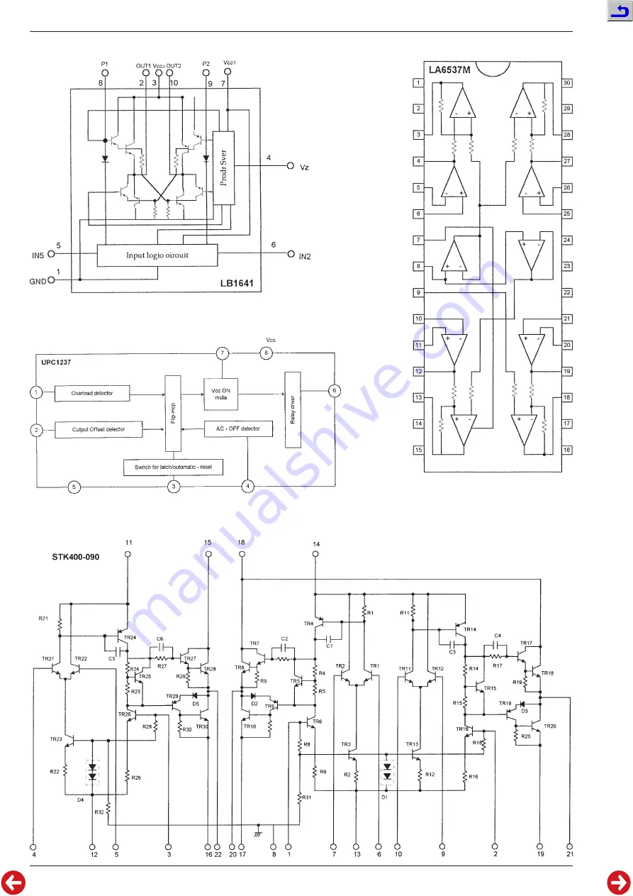
Page 36: ...3 31 GRUNDIG Service Schaltpl ne und Platinenabbildungen Circuit Diagrams and Layout of PCBs M 49 DPL IC703 IC704 LB1641 IC202 STK400 090 IC203 UPC1237HA IC702 LA6537...
Page 37: ...VCO FF 38KHz DECODER ST SW 6dB PILOT DET LED DRIVE FF 19KHz FF 19KHz 90 FM DET 23 12 15 14 17 20 18 19 25 16 4 GND SEP R OUT L OUT AM MUTE TU ST RESET AM FM AGC METER AM SO ADJ FM AFC OUT BU OUT SD AD...
Page 38: ...WALLOW COUNTER 1 16 1 17 4bits 12 bits PROGRAMMABLE DIVIDER 1 2 DATASHIFT REGISTER LATCH CCB I F 21 17 6 5 4 3 15 16 22 1 VSS VDO DO CL DI CE AM IN FM IN XOUT XIN 10 19 20 12 12 PO AIN AOUT IF IN 13 1...
Page 39: ...GRUNDIG Service 3 34 Schaltpl ne und Platinenabbildungen Circuit Diagrams and Layout of PCBs M 49 DPL IC308 LC75396E IC502 24C02...
Page 40: ...Buffer 4 3 State Buffer 5 3 State Buffer 6 3 State Buffer 7 3 State Buffer 8 11 12 13 14 7 6 5 Q2 Q3 Q4 Q5 Q6 Q7 Q8 10 9 Q QS S Clock Clock Clock Clock Clock Clock Clock Clock Strobe Strobe Strobe St...
Page 41: ...gen und Ersatzteillisten Exploded Views and Spare Parts Lists M 49 DPL M 49 DPL 3 36 4 1 U601 M51167BPF U602 UPC1330 U603 CXA1552 Explosionszeichnungen und Ersatzteillisten Exploded Views and Spare Pa...
Page 42: ...56 57 58 56 57 59 60 18 39 62 63 64 65 61 60 57 39 70 66 70 79 80 81 82 83 84 85 86 88 89 93 92 91 90 87 70 71 72 73 74 75 18 76 77 70 78 69 18 2 1 3 4 5 6 7 8 9 10 11 12 13 14 15 16 17 18 99 69 98 97...
Page 43: ...DRIVE BELT 0026 000 3 75955 006 8700 4 PUFFER CUSHION 0027 000 3 75955 006 7900 2 FEDER MD H SPRING MD H 0028 000 3 75955 006 9600 2 FEDER MD G SPRING MD G 0030 000 3 75955 006 8800 FEDER VERRIEGLUNG...
Page 44: ...FRONT PART 0088 000 1 75955 002 4500 2 GUMMI FUSS RUBBER FOOT 0089 000 1 75955 006 3400 ABDECKUNG GEH VORDERTEIL COVER CABINET FRONT BOTTO 0090 000 1 75955 002 4700 KNOPF LAUTSTAERKE KNOB VOLUME 0091...
Page 45: ...T 4 3MM SW 00520 75954 036 7700 TAKTSCHALTER 1P2T 4 3MM SW 00521 75954 036 7700 TAKTSCHALTER 1P2T 4 3MM SW 00522 75954 036 7700 TAKTSCHALTER 1P2T 4 3MM SW 00523 75954 036 7700 TAKTSCHALTER 1P2T 4 3MM...
Page 46: ...309 75955 006 2100 SMD IC LV1035M Q 00316 75954 021 2000 TRANS DTC 343 TS Q 00318 75954 021 2000 TRANS DTC 343 TS Q 00319 75987 361 5200 TRANS 2 SC 3330 UT Q 00320 75987 361 5200 TRANS 2 SC 3330 UT Q...