USB 3.0 Hub Design Guide
© 2015 Genesys Logic, Inc. - All rights reserved.
Page 21
GLI Confidential
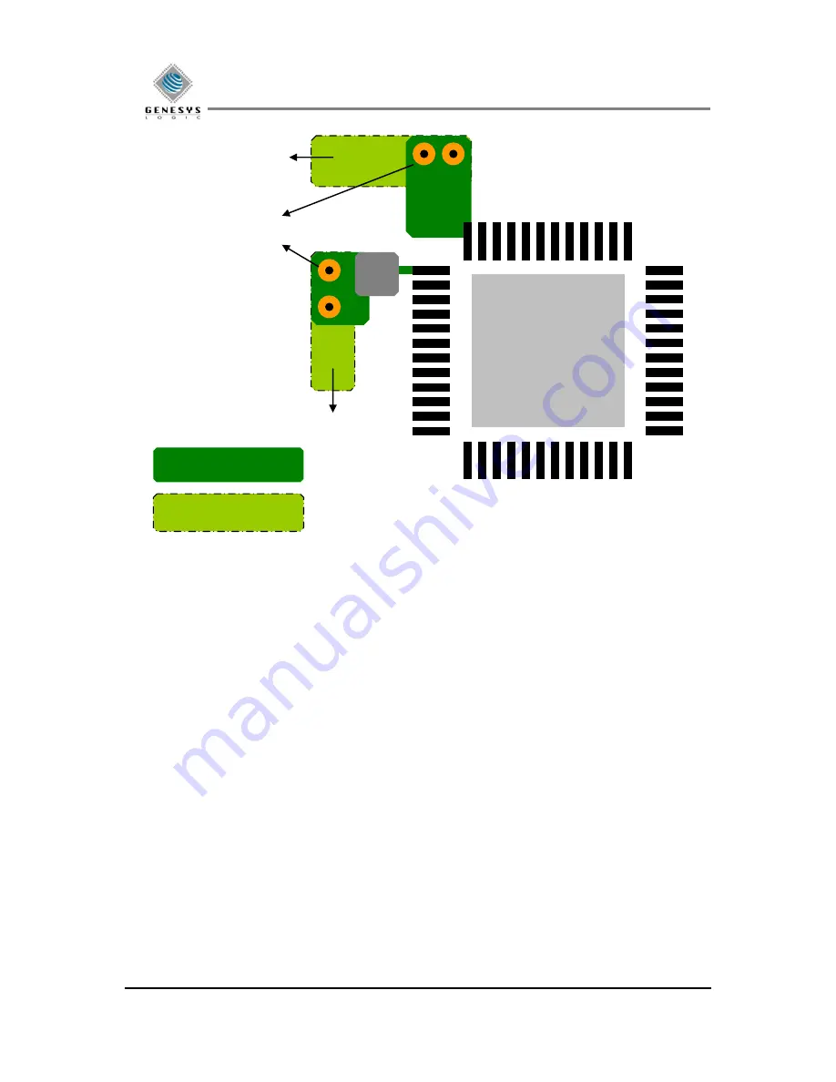
Figure 2.22
Bottom Layer:
1.2V power source to USB3.0 HUB
L1 Inductance
Top Layer: Minimum 2 via hole
Top layer Color
Bottom layer Color
Bottom Layer:
5V power source


