16 IPN250RTM
Publication No. IPN250RTM-HRM/2
NOTE
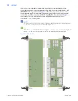
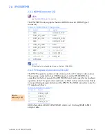
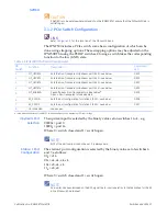
The IPN250 supports three x1 lane PCIe ports. However, there is insufficient space on the
IPN250RTM front panel to bring all three PCIe ports to connectors.
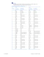
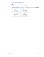
Table 2-4 IPN250RTMA J6 Pin Assignments
Pin
Number
Side B
Side A
Connector
Signal Name
IPN250RTM
Signal Name
Connector
Signal Name
IPN250RTM
Signal Name
1
GND Ground
GND
Ground
2
PERP0 PCIE1_RXP
PETP0 PCIE1_TXP
3
PERN0 PCIE1_RXN
PETN0 PCIE1_TXN
4
GND GND
GND GND
5
PERP1
100R link to B6
PETP1
100R link to A6
6
PERN1
100R link to B5
PETN1
100R link to A5
7
GND GND
GND GND
8
PERP2
100R link to B9
PETP2
100R link to A9
9
PERN2
100R link to B8
PETN2
100R link to A8
10
GND GND
GND
GND
11
PERP3
100R link to B12
PETP3
100R link to A12
12
PERN3
100R link to B11
PETN3
100R link to A11
13
GND GND
GND
GND
14
PWR
P3V3_AUX
CREFCLKP
100R link to A15
15
PWR
P3V3_AUX
CREFCLKN
100R link to A14
16
PWR
P3V3_AUX
GND GND
17
PWR_RTN
GND
RSVD
NC
18
PWR_RTN
GND RSVD
NC
19
PWR_RTN
GND
SB_RET
10kR link to P3V3_AUX
20
CWAKE~
10kR link to P3V3_AUX
CPRSNT
10kR link to P3V3_AUX
21
CPERST~
10kR link to P3V3_AUX
CPWRON
10kR link to P3V3_AUX
22
GND
GND GND
GND
23
PERP4
100R link to B24
PETP4
100R link to A24
24
PERN4
100R link to B23
PETN4
100R link to A23
25
GND GND
GND
GND
26
PERP5
100R link to B27
PETP5
100R link to A27
27
PERN5
100R link to B26
PETN5
100R link to A26
28
GND
GND
GND GND
29
PERP6
100R link to B30
PETP6
100R link to B30
30
PERN6
100R link to B29
PETN6
100R link to B29
31
GND
GND
GND GND
32
PERP7
100R link to B33
PETP7
100R link to A33
33
PERN7
100R link to B32
PETN7
100R link to A32
34
GND
GND
GND GND


