background image

2-3-3

D5P4HSMA

1-A. Preliminary/Final Checking and 

Alignment of Tape Path

Purpose:

To make sure that the tape path is well stabilized.

Symptom of Misalignment:

If the tape path is unstable, the tape will be damaged.

Note: Do not use an Alignment Tape for this proce-
dure. If the unit is not correctly aligned, the tape may
be damaged.

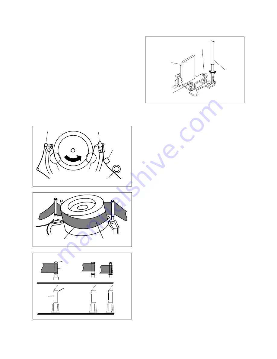
1. Playback a blank cassette tape and check to see

that the tape runs without creasing at Guide Rollers
[2] and [3], and at points A and B on the lead sur-
face. (Refer to Fig. M3 and M4.)

2. If creasing is apparent, align the height of the guide

rollers by turning the top of Guide Rollers [2] and
[3] with a Guide Roller Adj. Screwdriver. (Refer to
Fig. M3 and M5.)

3. Check to see that the tape runs without creasing at

Take-up Guide Post [4] or without snaking between
Guide Roller [3] and ACE Head. (Fig. M3 and M5)

4. If creasing or snaking is apparent, adjust the Tilt

Adj. Screw of the ACE Head. (Fig. M6)

1-B. X Value Alignment

Purpose: 

To obtain maximum PB FM envelope signal at the pre-
set position of the Tracking Control Circuit, align the
Horizontal Position of the ACE Head.

Symptom of Misalignment:

If the Horizontal Position of the ACE Head is not prop-
erly aligned, maximum PB FM envelope cannot be
obtained at the preset position of the Tracking Control
Circuit.

1. Connect the oscilloscope to TP301 (C-PB) and

TP503 (CTL) on the Main CBA. Use TP504 (RF-
SW) as a trigger.

2. Playback the Gray Scale of the Alignment Tape

(FL6NS8) and confirm that the PB FM signal is
present.

3. Set the Tracking Control Circuit to the preset posi-

tion by pressing CH UP button on the remote con-
trol unit then “PLAY” button on the unit. (Refer to
note on bottom of page 2-3-4.)

4. Use the Flat Screwdriver so that the PB FM signal

at TP301 (C-PB) is maximum. (Fig. M6)

Guide Roller [2]

Guide Roller [3]

A

B

Take-up Guide Post [4]

ACE Head

Fig. M3

Lead Surface of Cylinder

Tape

Fig. M4

Take-up Guide
Post

Tape

Guide Roller

Tape

Correct

Incorrect

Fig. M5

Azimuth Adj. Screw

Flat 
Screwdriver

Tilt Adj. Screw

ACE Head

Fig. M6

Summary of Contents for DPVR-5505

Page 1: ...ations I Preparation for Servicing I Adjustment Procedures I Schematic Diagrams I CBA s I Exploded views I Parts List Sec 2 Deck Mechanism Section I Standard Maintenance I Alignment for Mechanism I Disassembly Assembly of Mechanism I Alignment Procedures of Mechanism I Deck Exploded Views I Deck Parts List PAL ...

Page 2: ...1 9 1 Function Indicator Symbols 1 9 10 Schematic Diagrams CBA s and Test Points 1 10 1 Waveforms 1 11 1 Wiring Diagram VCR Section 1 12 1 Wiring Diagram DVD Section 1 12 2 IC Pin Function Descriptions 1 13 1 Lead Identifications 1 14 1 Exploded Views 1 15 1 Mechanical Parts List 1 16 1 Electrical Parts List 1 17 1 Sec 1 Main Section I Specifications I Preparation for Servicing I Adjustment Proced...

Page 3: ...O Burst 1 4 Video Color S N AM R P dB 37 41 SP Mode 1 5 Video Color S N PM R P dB 30 36 SP Mode 1 6 Resolution PB Line 230 245 SP Mode 2 Servo 2 1 Jitter Low µsec 0 07 0 12 SP Mode 2 2 Wow Flutter 0 3 0 5 SP Mode 3 Normal Audio 3 1 Output PB dBV 9 4 3 SP Mode 3 2 Output R P dBV 9 4 1 5 SP Mode 3 3 S N R P dB 36 41 SP Mode 3 4 Distortion R P 1 0 4 0 SP Mode 3 5 Freq resp R P at 200Hz dB 6 2 SP Mode...

Page 4: ...ad imp 100 k ohm 4 Ambient temperature 5 C 40 C ITEM CONDITIONS UNIT NOMINAL LIMIT 1 Video Output 75 ohm load Vpp 1 0 0 1 2 Optical Digital Out dBm 18 3 Audio PCM 3 1 Output Level 1 kHz 0 dB Vrms 2 0 3 2 S N dB 90 3 3 Freq Response DVD fs 48 kHz 0 5dB Hz 20 22 k CD fs 44 1 kHz 0 5dB Hz 20 20 k 3 4 THD N DVD 1 kHz 0dB 0 01 CD 1 kHz 0dB 0 01 ...

Page 5: ... eyes at least 30cm away from the pickup lens when the diode is turned on Do not look directly at the laser beam Caution Use of controls and adjustments or doing procedures other than those specified herein may result in hazardous radiation exposure Do not look directly at the laser beam coming from the pickup or allow it to strike against your skin Drive Mecha Assembly Laser Beam Radiation Laser ...

Page 6: ...te especially 1 Wires covered with PVC tubing 2 Double insulated wires 3 High voltage leads D Use specified insulating materials for hazardous live parts Note especially 1 Insulation tape 2 PVC tubing 3 Spacers 4 Insulators for transistors E When replacing AC primary side components transformers power cord etc wrap ends of wires securely about the terminals before solder ing F Observe that the wir...

Page 7: ...age Current Test Confirm the specified or lower leakage current between B earth ground power cord plug prongs and externally exposed accessible parts RF termi nals antenna terminals video and audio input and output terminals microphone jacks earphone jacks etc is lower than or equal to the specified value in the table below Measuring Method Power ON Insert load Z between B earth ground power cord ...

Page 8: ...machine then apply hot air to the Flat Pack IC about 5 to 6 seconds Fig S 1 1 2 Remove the flat pack IC with tweezers while apply ing the hot air 3 Bottom of the flat pack IC is fixed with glue to the CBA when removing entire flat pack IC first apply soldering iron to center of the flat pack IC and heat up Then remove glue will be melted Fig S 1 6 4 Release the flat pack IC from the CBA using twee...

Page 9: ... removing entire flat pack IC first apply soldering iron to center of the flat pack IC and heat up Then remove glue will be melted Fig S 1 6 4 Release the flat pack IC from the CBA using twee zers Fig S 1 6 With Iron Wire 1 Using desoldering braid remove the solder from all pins of the flat pack IC When you use solder flux which is applied to all pins of the flat pack IC you can remove it easily F...

Page 10: ... Installation 1 Using desoldering braid remove the solder from the foil of each pin of the flat pack IC on the CBA so you can install a replacement flat pack IC more easily 2 The I mark on the flat pack IC indicates pin 1 See Fig S 1 7 Be sure this mark matches the 1 on the PCB when positioning for installation Then presolder the four corners of the flat pack IC See Fig S 1 8 3 Solder all pins of ...

Page 11: ...ed to remove any static electricity that may be charged on the body 2 Ground for Workbench 1 Be sure to place a conductive sheet or copper plate with proper grounding 1MΩ on the workbench or other surface where the semi conductors are to be placed Because the static electricity charge on clothing will not escape through the body ground ing band be careful to avoid contacting semi con ductors with ...

Page 12: ...into the Deck Mechanism Assembly and press the PLAY button The tape will be loaded into the Deck Mechanism Assembly Make sure the power is on connect TP501 S INH to GND This will stop the function of Tape Start Sensor Tape End Sensor and Reel Sensors If these TPs are connected before plugging in the unit the function of the sensors will stay valid See Fig 1 Note Because the Tape End Sensors are in...

Page 13: ... ID LOC No PART REMOVAL Fig No REMOVE UNHOOK UNLOCK RELEASE UNPLUG DESOLDER Note 1 Top Case D1 8 S 1 2 Front Assembly D2 3 L 1 3 L 2 1 1 1 1 2 3 Top Bracket D2 3 S 2 4 DVD Mecha Assembly D3 4 S 3 CN401 CN601 5 Partition Plate D3 S 4 6 Power Suppy CBA D3 2 S 5 CN501 1 Top Case 2 Front Assembly 3 Top Bracket 4 DVD Mecha Assembly 8 DVD Main CBA 5 Partition Plate 7 Loader Holder 6 Power Supply CBA 9 V...

Page 14: ...t Fig D4 2 2 Short the three short lands of FPC cable with sol der before removing the FFC cable CN201 from it If you disconnect the FFC cable CN201 the laser diode of pickup will be destroyed Fig D4 CAUTION 3 When reassembling confirm the FFC cable CN201 is connected completely Then remove the solder from the three short lands of FPC cable Fig D4 4 When reassembling solder wire jumpers as shown i...

Page 15: ...n Plate 6 Power Supply CBA 7 Loader Holder 4 DVD Mecha Assembly Fig D3 CN201 CN301 S 7 S 7 8 DVD Main CBA DVD Mecha A Fig D4 Short the three short lands by soldering Either of two places Connector View for A S 8 S 9 S 9 S 8 S 8 L 3 9 VCR Chassis Unit Fig D5 S 10 S 10 ...

Page 16: ...BOTTOM VIEW Lead connections of Deck Assembly and Main CBA Desolder From Capstan Motor Assembly Printing side Desolder From Cylinder Assembly From ACE Head Assembly Lead with blue stripe Lead with blue stripe Desolder Lead with red stripe 13 Main CBA SW507 LD SW LD SW Pin Hole Hole Shaft Cam Gear 13 Main CBA 10 Deck Assembly Pin 12 Power SW CBA Desolder Lead with blue stripe Desolder Lead with blu...

Page 17: ...ew for A Rotate this roulette in the direction of the arrow A DVD Mecha HOW TO EJECT MANUALLY 1 Remove the Top Case 2 Rotate the roulette in the direction of the arrow as shown below 3 Pull the tray slowly with a hand ...

Page 18: ... Dual trace with 10 1 probe V Range 0 001 50V Div F Range DC AC 20MHz 2 Alignment Tape FL6A Head Switching Position Adjustment Purpose To determine the Head Switching position during playback Symptom of Misadjustment May cause Head Switching noise or vertical jitter in the picture Reference Notes Playback the Alignment tape and adjust VR501 so that the V sync front edge of the CH1 video output wav...

Page 19: ...er on by pressing the FUNCTION button and the tray will close 9 Press 1 2 3 4 and DISPLAY buttons on the remote control unit in that order Fig g appears on the screen 10 Press CLEAR button on the remote control unit Fig h appears on the screen When OK appears on the screen the factory default will be set Then the firmware renewal mode is complete 11 To exit this mode press FUNCTION button F W Vers...

Page 20: ... SENS INH CAPSTAN MOTOR IC501 SERVO SYSTEM CONTROL LINE MUTE LINE MUTE 28 5 6 SENSOR CBA SENSOR CBA END S ST S Q504 Q503 REC SAFETY END S CTL 97 TP503 CTL 82 TO DVD SYSTEM CONTROL BLOCK DIAGRAM DVD SECTION TO DVD SYSTEM CONTROL BLOCK DIAGRAM DVD SECTION CN502 C FG C CONT D PFG C F R 90 76 87 78 LM FWD REV 81 D CONT 77 AL 20 5V 12V AL 12V 2 P ON 15V P ON 5V 1 AL 20 5V 12V 2 P ON 5V 3 C FG 4 C F R 5...

Page 21: ...CCD 1H DELAY SP BYPASS MUTE PB EE IN1 TUNER IN1 TUNER MUTE PB EE FRT IN2 FRT IN2 AGC P R R Y C P R P R P EP Y DELAY Y C MIX 21 79 78 AGC VXO OSD CHARACTER MIX FBC 1 2 58 59 65 29 28 69 68 46 43 84 83 71 62 70 D REC H 80 BUFFER Q104 DVD VCR TP751 V OUT WF3 TP301 C PB WF2 TU VIDEO VIDEO MAIN CBA 54 TP504 RF SW WF1 OUTPUT SELECT DVD VIDEO TO SERVO SYSTEM CONTROL BLOCK DIAGRAM X301 4 43MHz C SYNC C SY...

Page 22: ...A OUT2 L JACK A CBA A IN2 5 5 A OUT2 1 1 CN2017 CN2018 JK101 A OUT1 R A OUT1 L 2 6 1 3 A IN1 R A IN1 L IC751 OUTPUT SELECT 12 13 14 15 2 1 11 10 9 SW CTL VCR DVD VCR DVD TO SERVO SYSTEM CONTROL BLOCK DIAGRAM OUTPUT SELECT DVD AUDIO SIGNAL REAR JK751 A OUT R A OUT L SW CTL 13 IC1404 INPUT SELECT 12 11 14 17 15 13 FRONT JK754 A IN TO SERVO SYSTEM CONTROL BLOCK DIAGRAM FRONT AV SW CTL IC151 SWITCHING...

Page 23: ...NER IN2 IN1 R ALC DET ALC IC301 AUDIO SIGNAL PROCESS 15 13 17 4 A PB REC CN504 3 A COM 1 AE H 2 AE H FE H AUDIO HEAD AUDIO ERASE HEAD AC HEAD ASSEMBLY FE HEAD 2 FE H 1 FE H GND CN501 MAIN CBA PB AUDIO SIGNAL REC AUDIO SIGNAL Mode SP REC 71 A MUTE H IIC BUS SCL IIC BUS SDA TO SERVO SYSTEM CONTROL BLOCK DIAGRAM FULL ERASE HEAD 68 69 SERIAL DECODER DECK ASSEMBLY 12 16 INV ATT Comparison Chart of Mode...

Page 24: ...IGNAL Mode SP REC DVD AUDIO SIGNAL AFV CBA JK101 A OUT1 R A OUT1 L 2 6 2 6 1 3 1 3 JK1402 A IN2 R A IN2 L A IN1 R A IN1 L A OUT2 R A OUT2 L TU AUDIO R 4 TU AUDIO L 5 4 5 CN701 CN1 SIF 2 2 CN701 CN1 TU701 TUNER UNIT SIF OUT AUDIO 22 2 ALC SW SW ALC 67 65 Q451 MUTE ON MUTE ON REAR TO DVD VIDEO AUDIO BLOCK DIAGRAM DVD SECTION FRONT JK751 Q753 Q754 A OUT R A OUT L JK754 A IN R JK753 A IN L IC751 OUTPU...

Page 25: ...9 F1 8 1 3 5 9 8 F2 FROM PIN 67 OF IC501 TO PIN 86 OF IC501 FROM PIN 66 OF IC501 CAUTION FOR CONTINUED PROTECTION AGAINST FIRE HAZARD REPLACE ONLY WITH THE SAME TYPE T1 6AL 250V FUSE NOTE The voltage for parts in hot circuit is measured using hot GND as a common terminal CAUTION Fixed voltage or Auto voltage selectable power supply circuit is used in this unit If Main Fuse F1001 is blown check to ...

Page 26: ... MICRO CONTROLLER SLED MOTOR DRIVE FOCUS ACTUATOR DRIVE SPINDLE MOTOR DRIVE TRACKING ACTUATOR DRIVE 147 TRAY IN SLD 75 SPDL 76 TRACKING DRIVE 148 FOCUS DRIVE TO DIGITAL SIGNAL PROCESS BLOCK DIAGRAM FS FS TS TS TO DVD VIDEO AUDIO BLOCK DIAGRAM 57 ADAC MD 56 ADAC MC 86 ADAC ML ADAC MC ADAC ML PCM SCLK 88 A MUTE ADAC MD A MUTE 163 PCM SCLK TRAY IN 3 SP 4 SP 5 TRAY IN 6 GND 7 SL 8 SL VREF RESET 73 RES...

Page 27: ... WATCH DOG TIMER CPU I F TIMER DECODER I F CPU I F READ MEMORY DATA RAM DSP DECODER I O PROCESSOR INST ROM DATA RAM INST ROM SERIAL D A GENERAL I O INTERRUPT CONTROLLER TIMER WATCH DOG TIMER REMOTE CONTROL 32BIT CPU STREAM I F EXTERNAL MEMORY I F SDRAM ECC UMAC 114 115 116 117 132 131 134 133 129 130 126 124 125 123 83 DEBUG BCU INST RAM DATA RAM D A D A D A TO DVD VIDEO AUDIO BLOCK DIAGRAM 156 15...

Page 28: ...LK ADAC MD ADAC MC ADAC ML PCM SCLK MAIN CBA DVD MAIN CBA UNIT DVD AUDIO SIGNAL DATA AUDIO SIGNAL 19 19 SPDIF A MUTE 3 3V Q1204 WF9 5 WF7 WF8 CN601 CN1601 1 1 VIDEO Y 10 10 VIDEO C 4 4 VIDEO R 8 8 VIDEO G 6 6 VIDEO B VIDEO Y VIDEO C VIDEO R VIDEO G FROM DIGITAL SIGNAL PROCESS BLOCK DIAGRAM DVD VIDEO SIGNAL VIDEO B TO Hi Fi AUDIO BLOCK DIAGRAM VCR SECTION 11 15 7 JK101 DVD G DVD R DVD B JK1401 S VI...

Page 29: ...ctly When the drum is not working properly P ON Power safety detection MODE INDICATOR ACTIVE When reel or capstan mechanism is not functioning correctly A R is displayed on a TV screen Refer to Fig 1 When tape loading mechanism is not func tioning correctly A T is displayed on a TV screen Refer to Fig 2 When cassette loading mechanism is not functioning correctly A C is displayed on a TV screen Re...

Page 30: ...itute replacement parts that do not have the same safety characteristics as speci fied in the parts list may create shock fire or other hazards Notes 1 Do not use the part number shown on these draw ings for ordering The correct part number is shown in the parts list and may be slightly different or amended since these drawings were prepared 2 All resistance values are indicated in ohms K 103 M 10...

Page 31: ...its use only original replacement parts which are listed with their part numbers in the parts list section of the service manual 4 Voltage indications for PLAY and REC modes on the schematics are as shown below 5 How to read converged lines 6 Test Point Information 2 3 1 5 0 2 5 PLAY mode STOP mode 5 0 The same voltage for both PLAY STOP modes Indicates that the voltage is not consistent here DVD ...

Page 32: ...1 10 3 1 10 4 H9776SCM1 Main 1 8 Schematic Diagram VCR Section Comparison Chart of Models and Marks MODEL MARK DPVR 5505 A DPVR 5505V B DPVR 5805 C ...

Page 33: ...P VCR CHP REC SACD TRK A ALL B PSCAN DVD PM HDVCD A 7G 6G 5G 4G 3G 2G 1G a b c d e f g c d e f f g c d e f g c d e f g c d e f g c d e f g h i i a b a b a b a b a b IC611 MATRIX CHART REPEAT TITLE GROUP VCR CHP REC SACD TRK ALL B PSCAN DVD P M HD V CD A A Comparison Chart of Models and Marks MODEL MARK DPVR 5505 A DPVR 5505V B DPVR 5805 C ...

Page 34: ...Main 3 8 Schematic Diagram VCR Section 1 10 7 1 10 8 H9776SCM3 Comparison Chart of Models and Marks MODEL MARK DPVR 5505 A DPVR 5505V B DPVR 5805 C ...

Page 35: ...Main 4 8 Schematic Diagram VCR Section 1 10 9 1 10 10 H9776SCM4 ...

Page 36: ...1 10 11 1 10 12 H9776SCM5 Main 5 8 Schematic Diagram VCR Section Comparison Chart of Models and Marks MODEL MARK DPVR 5505 A DPVR 5505V B DPVR 5805 C ...

Page 37: ...Main 6 8 Schematic Diagram VCR Section 1 10 13 1 10 14 H9776SCM6 Comparison Chart of Models and Marks MODEL MARK DPVR 5505 A DPVR 5505V B DPVR 5805 C ...

Page 38: ...ction 1 10 15 1 10 16 H9776SCM7 Comparison Chart of Models and Marks MODEL MARK DPVR 5505 A DPVR 5505V B DPVR 5805 C PIN NAME 1 4 CHART MODEL MARK PLAY FP CLK SKIP DOWN FP DIN DISC IN FP STB SKIP UP FP DOUT PIN NAME MAY DIFFER BY MODELS 2 3 4 C A B 1 ...

Page 39: ...Main 8 8 Schematic Diagram C VCR Section 1 10 17 1 10 18 H9778SCM8 Comparison Chart of Models and Marks MODEL MARK DPVR 5505 A DPVR 5505V B DPVR 5805 C ...

Page 40: ...ith the same type fuse CAUTION Fixed voltage or Auto voltage selectable power supply circuit is used in this unit If Main Fuse F1001 is blown check to see that all components in the power supply circuit are not defective before you connect the AC plug to the AC power supply Otherwise it may cause some components in the power supply circuit to fail Comparison Chart of Models and Marks MODEL MARK DP...

Page 41: ...Jack A Schematic Diagram VCR Section 1 10 21 1 10 22 H9776SCJ Comparison Chart of Models and Marks MODEL MARK DPVR 5505 A DPVR 5505V B DPVR 5805 C ...

Page 42: ...AFV Schematic Diagram C VCR Section 1 10 23 1 10 24 H9778SCAFV Comparison Chart of Models and Marks MODEL MARK DPVR 5505 A DPVR 5505V B DPVR 5805 C ...

Page 43: ...V OUT TP751 WF3 C PB TP301 WF2 SW P VR501 CTL TP503 RF SW TP504 WF1 S INH TP501 Main CBA Sensor CBA Top View BHF300F01011A BHF300F01011B Sensor CBA Top View 1 10 25 1 10 26 BH9700F01016A ...

Page 44: ...PIN14OF CN1601 WF5 PIN 10 OF CN1601 WF4 PIN 1 OF CN1601 WF8 PIN 16 OF CN1601 WF6 PIN 6 OF IC1403 WF9 PIN 19 OF CN1601 WF7 Main CBA Bottom View BH9700F01016A 1 10 27 1 10 28 ...

Page 45: ...1 10 29 1 10 30 BH9700F01016C DVD Open Close CBA Top View DVD Open Close CBA Bottom View Power SW CBA Top View Power SW CBA Bottom View BH9700F01016B ...

Page 46: ...31 1 10 32 Jack A CBA Top View Jack A CBA Bottom View BH9700F01022C AFV CBA Top View C AFV CBA Bottom View C BHC400F01093 Comparison Chart of Models and Marks MODEL MARK DPVR 5505 A DPVR 5505V B DPVR 5805 C ...

Page 47: ...TROUBLESHOOTING THIS TYPE POWER SUPPLY CIRCUIT A VARIABLE ISOLATION TRANSFORMER IS REQUIRED CAUTION Fixed voltage or Auto voltage selectable power supply circuit is used in this unit If Main Fuse F1001 is blown check to see that all components in the power supply circuit are not defective before you connect the AC plug to the AC power supply Otherwise it may cause some components in the power supp...

Page 48: ...matic Diagram DVD Section Comparison Chart of Models and Marks MODEL MARK DPVR 5505 A DPVR 5505V B DPVR 5805 C PIN NAME 1 4 CHART MODEL MARK PLAY FP CLK SKIP DOWN FP DIN DISC IN FP STB SKIP UP FP DOUT PIN NAME MAY DIFFER BY MODELS 2 3 4 C A B 1 ...

Page 49: ...matic Diagram DVD Section Comparison Chart of Models and Marks MODEL MARK DPVR 5505 A DPVR 5505V B DPVR 5805 C PIN NAME 1 4 CHART MODEL MARK PLAY FP CLK SKIP DOWN FP DIN DISC IN FP STB SKIP UP FP DOUT PIN NAME MAY DIFFER BY MODELS 2 3 4 C A B 1 ...

Page 50: ...2 125 0 3 0 1 30 61 A B 0 0 93 0 0 126 0 1 0 1 31 61 C 3 5 3 5 94 127 2 3 2 3 32 62 3 4 3 4 95 128 1 7 1 7 33 63 0 0 96 129 2 3 2 3 PIN NO PLAY STOP PIN NO PLAY STOP PIN NO PLAY STOP PIN NO PLAY STOP 130 2 3 2 3 163 1 8 1 8 196 3 4 3 4 229 0 0 131 2 3 2 3 164 0 0 197 230 132 2 4 2 3 165 1 7 1 8 198 231 3 4 3 4 133 2 4 2 4 166 1 7 1 7 199 232 1 3 1 6 134 2 4 2 4 167 3 4 3 4 200 233 135 2 3 2 3 168 ...

Page 51: ...1 10 41 1 10 42 H9776SCD3 DVD Main 3 3 Schematic Diagram DVD Section ...

Page 52: ... 6 of IC1403 WF5 VIDEO Y VIDEO Y 0 2V 0 2V 20 20µs VIDEO C VIDEO C 0 2V 0 2V 20 20µs DVD VIDEO DVD VIDEO 0 5V 0 5V 20 20µs WF7 DVD A L DVD A L 1V 1V 0 5ms 0 5ms WF8 DVD A R DVD A R 1V 1V WF9 SPDIF SPDIF 1V 1V 0 1 0 1µs s Pin 1 of CN1601 Pin 10 of CN1601 Pin 14 of CN1601 Pin 16 of CN1601 Pin 19 of CN1601 NOTE Input VCR COLOR BAR SIGNAL WF1 WF3 DVD POWER ON STOP MODE WF4 WF6 CD 1kHz PLAY WF7 WF9 0 5...

Page 53: ... 27 OUTPUT SELECT DVD PLAY VIDEO R I P SW NU 1 VIDEO Y ASPECT VIDEO B GND GND VIDEO G GND VIDEO C GND GND DVD A L DVD A R MUTE DVD A R DVD A MUTE AUDIO 5V AUDIO 5V SPDIF TO WIRING DIAGRAM DVD SECTION AFV CBA DVD OPEN CLOSE CBA SIF 1 NU 2 TU AUDIO R 3 GND 4 TU AUDIO L 5 P ON 5V 6 P ON 5V 7 IIC BUS SCL 8 IIC BUS SDA 9 1 2 3 4 5 6 7 8 9 CN701 CN1 DVD OPEN CLOSE 1 EV 3 3V 2 1 2 CN2015 CN2016 JW008 CN5...

Page 54: ...8 19 20 TS TS FS CD LD FS GND DVD PD GND CD PD PD MONI DVD LD VREF E GND B P ON 5V CD DVD D A C F GND LD DETECTOR FS TS 7 9 11 2 3 6 5 4 TO WIRING DIAGRAM VCR SECTION 3 SP 4 SP 5 TRAY IN 6 GND 7 SL 8 SL 1 2 3 4 5 6 7 8 9 10 11 12 13 14 15 16 17 18 19 20 21 22 EV 1 2V EV 1 2V EV 3 3V EV 3 3V EV 3 3V P ON 3 3V P ON 5V EV 11V EV 11V GND GND GND GND GND GND GND PWRCON REMOTE DVD 23 24 25 26 DVD POWER ...

Page 55: ... Output H Hi z 14 IN REMOTE VIDEO Remote Control Sensor L 15 OUT C ROTA Color Phase Rotary Changeover SIgnal H L 16 OUT H A SW Video Head Amp Switching Pulse H L 17 IN H A COMP Head Amp Comparator Signal H L 18 OUT RF SW Video Head Switching Pulse H L 19 A B NU Not Used C OUT Hi Fi H SW HiFi Audio Head Switching Pulse H L 20 A B OUT FRONT AV Front AV Output Signal H L C NU Not Used 21 OUT DVD POWE...

Page 56: ... L Pin No Mark IN OUT Signal Name Function Active Level 60 OUT 8POUT 2 Control SCART 1 8Pin Level by using 8POUT 1 and 8POUT 2 Hi z L 61 NU Not Used 62 A B OUT AUDIO SW1 Audio IN OUT Control Signal H L C NU Not Used 63 A B OUT AUDIO SW2 Audio IN OUT Control Signal H L C NU Not Used 64 NU Not Used 65 NU Not Used 66 OUT C POW SW Capstan Power Switching Signal H L 67 OUT P ON H Power On Signal at Hig...

Page 57: ...for CTL AMP 93 P80 C P80 C Terminal 94 IN OUT CTL Playback RecordControl Signal H L 95 IN OUT CTL Playback RecordControl Signal H L 96 AMPC CTL AMP Connected Terminal 97 CTLAMP out To Monitor for CTL AMP Output PULSE 98 AMPVcc AMPVcc 99 AVcc A D Converter Power Input Standard Voltage Input 100 IN AGC IF AGC Comparator Signal A D Pin No Mark IN OUT Signal Name Function Active Level Pin No IN OUT Si...

Page 58: ... CD4052BCSJX CD4052BNSR CD4053BCSJX CD4053BNSR TC4052BF EL TC4053BF N 1 MID 32A22F PT204 6B 12 E C 35 7 BT 298N 7 BT 298NY 1 5 4 8 1 BR24L02F WE2 CAT24WC02JI 28 15 14 PT6313 S TP 1 0C 0805T 002 GP1FA513TZ 1 2 3 B1 E B2 C1 C2 FMG4A T148 RN1511 TE85R FA1F4M T1B KRC103S RTK KTC3875Y RTK C B E 60 LA72648M MPB E 21 40 41 20 1 80 61 16 9 8 1 MM1637XVBE 1 2 3 3 4 5 PQ070XZ5MZP 1 Vin 2 Vc 3 Vo 4 Vadj 5 GN...

Page 59: ...02 JW001 CN3001 CN3002 2L091 2L012 2L054 2B55 B AFV CBA Main CBA Jack A CBA Power Supply CBA Junction CBA 2L021 F1001 A B A A3 A7 2B5 2L012 2L041 2L041 2L041 2L041 2L041 2L041 A2 2L041 2L041 2B18 2B16 2B46 A22 A22 See Electrical Parts List for parts with this mark Some Ref Numbers are not in sequence A10 2L020 2B54 2L012 2L020 2L020 2B15 2B15 DPVR 5805 DPVR 5505 DPVR 5505V DPVR 5505 DPVR 5505V A1X...

Page 60: ...1 15 3 H9776PEX Packing S1 X4 Unit S3 S2 S2 X5 S7 Some Ref Numbers are not in sequence X2 X3 X1 A14 X20D X20C X20B X20A X20 DPVR 5505V DPVR 5805 X22 DPVR 5505 ...

Page 61: ...CASE HC460ED 0VM412906 2B40 PARTITION PLATE H9700ED 0VM306765 2B54 PLATE GROUND RCA H9700ED 0VM306867 2B55 PLATE GROUND 21P H9700ED 0VM416444 2L011 P TIGHT SCREW 3X8 BIND GBMP3080 2L012 SCREW S TIGHT M3X6 BIND HEAD GBMS3060 2L020 P TIGHT SCREW 3X8 BIND GBMP3080 2L021 SCREW P TIGHT 3X12 BIND HEAD GBMP3120 2L022 P TIGHT SCREW 3X8 BIND GBMP3080 2L041 SCREW P TIGHT 3X6 BIND HEAD GBCP3060 2L051 SCREW P...

Page 62: ...P 100µF 16V M CE1CMASTL101 C107 ELECTROLYTIC CAP 470µF 6 3V M or CE0KMASDL471 ELECTROLYTIC CAP 470µF 6 3V M CE0KMASTL471 C109 C CHIP CERAMIC CAP 1608 CH J 470pF 50V or CHD1JJ3CH471 C CHIP CERAMIC CAP CG J 470pF 50V CHD1JJ3CG471 C112 CHIP CERAMIC CAP 1608 CH J 470pF 50V or CHD1JJ3CH471 CHIP CERAMIC CAP CG J 470pF 50V CHD1JJ3CG471 C113 CHIP CERAMIC CAP 1608 F Z 0 1µF 50V or CHD1JZ30F104 CHIP CERAMIC...

Page 63: ...AP 1608 B K 0 01µF 50V CHD1JK30B103 C315 CHIP CERAMIC CAP 1608 B K 0 047µF 50V or CHD1JK30B473 Ref No Mark Description Part No CHIP CERAMIC CAP 1608 B K 0 047µF 25V CHD1EK30B473 C316 ELECTROLYTIC CAP 1µF 50V M H7 CE1JMAVSL1R0 C317 CHIP CERAMIC CAP 1608 F Z 0 1µF 50V or CHD1JZ30F104 CHIP CERAMIC CAP 1608 F Z 0 1µF 25V or CHD1EZ30F104 CHIP CERAMIC CAP FZ Z 0 1µF 50V CHD1JZ3FZ104 C319 CHIP CERAMIC CA...

Page 64: ...AMIC CAP CG J 220pF 50V CHD1JJ3CG221 C429 A B CHIP CERAMIC CAP 1608 CH J 68pF 50V or CHD1JJ3CH680 Ref No Mark Description Part No A B CHIP CERAMIC CAP CG J 68pF 50V CHD1JJ3CG680 C451 C CHIP CERAMIC CAP 1608 F Z 0 1µF 50V or CHD1JZ30F104 C CHIP CERAMIC CAP 1608 F Z 0 1µF 25V or CHD1EZ30F104 C CHIP CERAMIC CAP FZ Z 0 1µF 50V CHD1JZ3FZ104 C452 C ELECTROLYTIC CAP 10µF 16V M H7 CE1CMAVSL100 C453 C ELEC...

Page 65: ...CAP 1608 B K 4700pF 50V CHD1JK30B472 C533 CHIP CERAMIC CAP 1608 B K 0 047µF 50V or CHD1JK30B473 Ref No Mark Description Part No CHIP CERAMIC CAP 1608 B K 0 047µF 25V CHD1EK30B473 C534 ELECTROLYTIC CAP 47µF 6 3V M H7 CE0KMAVSL470 C535 CHIP CERAMIC CAP 1608 F Z 0 1µF 50V or CHD1JZ30F104 CHIP CERAMIC CAP 1608 F Z 0 1µF 25V or CHD1EZ30F104 CHIP CERAMIC CAP FZ Z 0 1µF 50V CHD1JZ3FZ104 C538 CHIP CERAMIC...

Page 66: ...CERAMIC CAP 1608 F Z 0 1µF 25V or CHD1EZ30F104 CHIP CERAMIC CAP FZ Z 0 1µF 50V CHD1JZ3FZ104 C1246 CHIP CERAMIC CAP 1608 F Z 0 1µF 50V or CHD1JZ30F104 Ref No Mark Description Part No CHIP CERAMIC CAP 1608 F Z 0 1µF 25V or CHD1EZ30F104 CHIP CERAMIC CAP FZ Z 0 1µF 50V CHD1JZ3FZ104 C1247 ELECTROLYTIC CAP 470µF 16V M or CE1CMASDL471 ELECTROLYTIC CAP 470µF 16V M CE1CMASTL471 C1249 ELECTROLYTIC CAP 47µF ...

Page 67: ... 7733D QDTD00MTZJ33 D1031 PCB JUMPER D0 6 P5 0 JW5 0T D1052 RECTIFIER DIODE 1N4005 or NDQZ001N4005 RECTIFIER DIODE 1N4005 NDWZ001N4005 D1053 RECTIFIER DIODE 1N4005 or NDQZ001N4005 Ref No Mark Description Part No RECTIFIER DIODE 1N4005 NDWZ001N4005 D1054 RECTIFIER DIODE 1N4005 or NDQZ001N4005 RECTIFIER DIODE 1N4005 NDWZ001N4005 D1057 RECTIFIER DIODE 1N4005 or NDQZ001N4005 RECTIFIER DIODE 1N4005 NDW...

Page 68: ...NSISTOR FMG4A T148 or QQ2Z000FMG4A CHIP TRANSISTOR RN1511 TE85R QQ2Z00RN1511 Ref No Mark Description Part No Q403 TRANSISTOR KTC3203 Y or NQSY0KTC3203 TRANSISTOR 2SC2120 Y TPE2 QQSY02SC2120 Q404 TRANSISTOR KTA1266 GR or NQS40KTA1266 TRANSISTOR 2SA1015 GR TPE2 QQS102SA1015 Q405 RES BUILT IN TRANSISTOR KRA103M or NQSZ0KRA103M RES BUILT IN TRANSISTOR BN1F4M T QQSZ00BN1F4M Q406 CHIP TRANSISTOR KTC3875...

Page 69: ...W J 1 2k Ω RCX4JATZ0122 R061 CARBON RES 1 4W J 8 2k Ω RCX4JATZ0822 R062 CHIP RES 1608 1 10W J 180 Ω RRXAJR5Z0181 R064 CARBON RES 1 4W J 8 2k Ω RCX4JATZ0822 R065 CHIP RES 1608 1 10W J 22k Ω RRXAJR5Z0223 R070 CARBON RES 1 4W J 820 Ω RCX4JATZ0821 R071 A B CARBON RES 1 4W J 270 Ω RCX4JATZ0271 R072 CARBON RES 1 6W J 1 Ω or RCX6JATZ01R0 CARBON RES 1 4W J 1 Ω RCX4JATZ01R0 R105 A B CARBON RES 1 6W J 4 7k ...

Page 70: ...1 10W 0 Ω RRXAZR5Z0000 R451 C CHIP RES 1608 1 10W J 8 2k Ω RRXAJR5Z0822 Ref No Mark Description Part No R452 C CHIP RES 1608 1 10W J 39k Ω RRXAJR5Z0393 R453 C CHIP RES 1608 1 10W J 5 6k Ω RRXAJR5Z0562 R454 C CHIP RES 1608 1 10W J 39k Ω RRXAJR5Z0393 R455 C CHIP RES 1608 1 10W J 5 6k Ω RRXAJR5Z0562 R456 C CHIP RES 1608 1 10W J 39k Ω RRXAJR5Z0393 R457 C CHIP RES 1608 1 10W J 5 6k Ω RRXAJR5Z0562 R458 ...

Page 71: ... 1 10W 0 Ω RRXAZR5Z0000 R622 C CHIP RES 1608 1 10W 0 Ω RRXAZR5Z0000 R623 C CHIP RES 1608 1 10W 0 Ω RRXAZR5Z0000 Ref No Mark Description Part No R624 C CHIP RES 1608 1 10W J 10k Ω RRXAJR5Z0103 R703 CARBON RES 1 6W J 1 8k Ω or RCX6JATZ0182 CARBON RES 1 4W J 1 8k Ω RCX4JATZ0182 R704 CHIP RES 1608 1 10W J 1k Ω RRXAJR5Z0102 R705 CHIP RES 1608 1 10W J 1k Ω RRXAJR5Z0102 R706 CARBON RES 1 4W J 1k Ω RCX4JA...

Page 72: ...r SST0101HH013 TACT SWITCH SKQSAF001A or SST0101AL041 TACT SWITCH TC 1104 H 9 5 SST0101DNG01 SW504 TACT SWITCH KSM0614B or SST0101HH013 TACT SWITCH SKQSAF001A or SST0101AL041 Ref No Mark Description Part No TACT SWITCH TC 1104 H 9 5 SST0101DNG01 SW506 LEAF SWITCH MXS01830MVP0 SSC0101MCE03 SW507 ROTARY MODE SWITCH SSS 53MD SSR0106KB003 SW601 TACT SWITCH KSM0614B or SST0101HH013 TACT SWITCH SKQSAF00...

Page 73: ...1µF 50V CHD1JZ3FZ104 C022 ELECTROLYTIC CAP 470µF 35V M or CE1GMASDL471 ELECTROLYTIC CAP 470µF 35V M CE1GMASTL471 C1001 METALLIZED FILM CAP 0 068µF 275V K or CT2E683HJE06 METALLIZED FILM CAP 0 068µF 250V K or CT2E683DC011 METALLIZED FILM CAP 0 068µF 250V K or CT2E683DC014 METALLIZED FILM CAP 0 068µF 250V M CT2E683MS037 C1004 ELECTROLYTIC CAP 100µF 400V M CA2H101S6016 C1005 CERAMIC CAP SL K 56pF 1KV...

Page 74: ...01 Ref No Mark Description Part No TRANSISTORS Q1001 FET 2SK3566 QFWZ02SK3566 Q1003 TRANSISTOR 2SC1815 GR TPE2 QQS102SC1815 Q1004 TRANSISTOR KTA1267 GR or NQS10KTA1267 TRANSISTOR KTA1267 Y or NQQY0KTA1267 TRANSISTOR 2SA1175 J or QQSJ02SA1175 TRANSISTOR 2SA1175 H or QQSH02SA1175 TRANSISTOR 2SA1175 F QQSF02SA1175 Q1008 TRANSISTOR KTC3199 Y or NQSY0KTC3199 TRANSISTOR KTC3199 GR or NQS10KTC3199 TRANSI...

Page 75: ...11BS ZENER DIODE MTZJT 7711A QDTA00MTZJ11 Ref No Mark Description Part No COIL L102 BEAD CORE B16 RH 3 5X10X1 3 XL03010XM001 TRANSISTORS Q103 TRANSISTOR KTA1266 GR or NQS40KTA1266 TRANSISTOR 2SA1015 GR TPE2 QQS102SA1015 RESISTORS R110 A B CARBON RES 1 6W J 4 7k Ω or RCX6JATZ0472 A B CARBON RES 1 4W J 4 7k Ω RCX4JATZ0472 R111 CARBON RES 1 6W J 220 Ω or RCX6JATZ0221 CARBON RES 1 4W J 220 Ω RCX4JATZ0...

Page 76: ...NNECTOR CN1 C ANGLE PIN HEADER 9P 6029B 1 09Z003 T 5700069 DIODES D2 C SWITCHING DIODE 1N4148M or NDTZ01N4148M C SWITCHING DIODE 1SS133 T 77 QDTZ001SS133 ICS IC1 C IC AUDIO PROCESSOR MSP3417G QG B8 or NSZBA0SP3002 C IC AUDIO PROCESSOR MSP3417G QG B8 V3 NSZBA0SP3005 COILS L1 C INDUCTOR 10µH K 26T LLAXKATTU100 L2 C PCB JUMPER D0 6 P5 0 JW5 0T L3 C INDUCTOR 18µH K 26T LLAXKATTU180 L4 C INDUCTOR 10µH ...

Page 77: ... Tools 2 2 1 Mechanical Alignment Procedures 2 3 1 Disassembly Assembly Procedures of Deck Mechanism 2 4 1 Alignment Procedures of Mechanism 2 5 1 Deck Exploded Views 2 6 1 Deck Parts List 2 7 1 Sec 2 Deck Mechanism Section I Standard Maintenance I Mechanism Alignment Procedures I Disassembly Assembly of Mechanism I Deck Exploded Views I Deck Parts List ...

Page 78: ...l DECK ADJUSTMENTS 3 For the reference numbers listed above refer to Deck Exploded Views B73 Recording model only B86 Not used in 2 head model h Hours Cleaning I Replace Deck Periodic Service Schedule Ref No Part Name 1 000 h 2 000 h 3 000 h 4 000 h B2 Cylinder Assembly I I B3 Loading Motor Assembly I B8 Pulley Assembly I I B587 Tension Lever Assembly I I B31 ACE Head Assembly I B573 B574 Reel S R...

Page 79: ... hard material but since it is very thin avoid cleaning it vertically 2 Wait for the cleaned part to dry thoroughly before operating the unit 3 Do not reuse a stained head cleaning stick or a stained chamois cloth Cleaning of ACE Head Clean the head with a cotton swab Procedure 1 Remove the top cabinet 2 Dip the cotton swab in 90 isopropyl alcohol and clean the ACE Head Be careful not to damage th...

Page 80: ...2 Alignment Tape FL6N8 2 Head model FL6NS8 4 Head model Azimuth and X Value Adjustment of ACE Head Adjustment of Envelope Waveform J 2 Guide Roller Adj Screwdriver Available Locally Guide Roller J 3 Mirror Available Locally Tape Transportation Check J 4 Azimuth Adj Screwdriver Available Locally ACE Head Height J 5 Flat Screwdriver Available Locally X Value ...

Page 81: ... that the Moving guide preparations are in the Eject Position 4 Turn the LDG Belt in the appropriate direction shown in Fig M1 until the Moving guide prepara tions come to the Eject Position Stop turning when the preparations begin clicking or can not be moved further However the tape will be left wound around the cylinder 5 Turn the LDG Belt in the appropriate direction con tinuously and the cass...

Page 82: ...here is no slack on the supply and take up side Guide Rollers Use a blank tape Adjust the height of the Guide Rollers Supply side and take up side Use a blank tape Page 2 3 3 Loading Use a blank tape Adjust the envelope Page 2 3 4 Check the envelope Adjust the Audio Section Azimuth Alignment Page 2 3 4 Check the audio output Check the following 1 X Value Page 2 3 3 2 Envelope Page 2 3 4 Adjust the...

Page 83: ...e ACE Head Fig M6 1 B X Value Alignment Purpose To obtain maximum PB FM envelope signal at the pre set position of the Tracking Control Circuit align the Horizontal Position of the ACE Head Symptom of Misalignment If the Horizontal Position of the ACE Head is not prop erly aligned maximum PB FM envelope cannot be obtained at the preset position of the Tracking Control Circuit 1 Connect the oscillo...

Page 84: ...ecomes as flat as possible To do this adjust ment turn the top of the Guide Roller with the Guide Roller Adj Screwdriver 3 If the envelope is as shown in Fig M7 adjust the height of Guide Roller 2 Refer to Fig M3 so that the waveform looks like the one shown in Fig M9 4 If the envelope is as shown in Fig M8 adjust the height of Guide Roller 3 Refer to Fig M3 so that the waveform looks like the one...

Page 85: ...of pushes to ensure preset position The number of pushes CH UP button to achieve 1 2 level of envelope should match the number of pushes CH DOWN button from center If required redo the X Value Alignment 1 E Checking and Alignment of Tape Path during reversing Purpose To make sure that the tape path is well stabilized dur ing reversing Symptom of Misalignment If the tape path is unstable during rev...

Page 86: ...ssembly T DM1H DM7H Desolder LDG Belt 2 S 3 9 9 ACE Head Assembly T DM1H DM7H S 4 10 2 Tape Guide Arm Assembly T DM1H DM8H 1 P 2 11 10 C Door Opener T DM1H DM8H 1 S 4A L 4 12 11 Pinch Arm B T DM1H DM8H 1 DM8H 2 P 3 13 12 Pinch Arm A Assembly T DM1H DM8H 1 DM8H 2 14 14 FE Head T DM1H DM9H S 5 15 15 Prism T DM1H DM9H S 6 16 2 Slider Shaft T DM10H L 5 17 16 C Drive Lever SP T DM10H 18 16 C Drive Leve...

Page 87: ...T Arm B DM2H DM14H P 5 34 26 Loading Arm SP Assembly B DM2H DM14H Refer to Alignment Sec Page 2 5 1 35 34 Loading Arm TU Assembly B DM2H DM14H Refer to Alignment Sec Page 2 5 1 36 16 26 M Brake TU Assembly HI T DM1H DM15H 37 2 26 M Brake SP Assembly HI T DM1H DM15H P 6 38 37 Tension Lever Assembly T DM1H DM15H 39 38 T Lever Holder T DM15H L 10 40 40 M Gear HI T DM1H DM15H C 6 41 15 40 Sensor Gear ...

Page 88: ...2 4 3 U29PHSDA 14 13 11 10 12 7 49 8 32 43 41 40 31 42 45 44 46 9 36 15 38 37 Fig DM1H Top View 34 19 35 25 26 24 23 27 33 20 28 22 Fig DM2H Bottom View ...

Page 89: ... Fig DM4H Pull up Slide 1 2 A 3 6 6 L 2 Pin A Hole A Pin B Hole B L 1 First insert 6 diagonally in 3 as shown below Then install 6 in 3 while pushing L 1 in a direction of arrow After installing 6 in 3 confirm that pin A of 3 enters hole A of 6 properly Installation of 3 and 6 View for A 2 1 4 Install 6 in 4 while pulling L 2 in a direction of arrow After installing 6 in 4 confirm that pin B of 4 ...

Page 90: ...th White Stripe A 8 Fig DM7H 11 13 12 10 L 4 P 3 P 2 Fig DM8H 1 Pin of 12 Pin of 10 Groove of 27 View for A When reassembling 10 and 12 confirm that pin of 10 and pin of 12 are in the groove of 27 as shown 27 Removal of 11 1 Remove screw S 4A 2 Unhook spring P 2 3 Release L 4 while holding 12 with a finger 4 Loosen a finger holding 12 and remove 11 A S 4A ...

Page 91: ...r to Fig A Fig A 13 12 P 3 Fig B Top view Install pin of 12 in groove of 27 Refer to Fig B 27 Hold 12 and 13 till groove of pin of chassis looks and fit 13 in notch of chassis Then turn a few 13 while holding 12 Refer to Fig C Fig C Groove of pin of chassis Notch of chassis turn 13 12 Install 11 and 10 while holding 12 Refer to Fig DM8H 1 Fig DM8H 2 14 15 S 6 S 5 Fig DM9H 17 16 L 5 18 P 4 S 7 Fig ...

Page 92: ...2 4 7 U29PHSDA 19 Cap Belt S 8 19 20 Cap Belt A Installation position of Cap Belt View for A Fig DM11H L 6 22 20 C 1 21 27 Pin on 22 Position of pin on 22 turn Fig DM12H ...

Page 93: ...n 47 First groove on 27 Align 26 and 27 as shown Pin of 36 Pin of 33 Position of Mode Lever when installed Pin of 37 Bottom View Installation of 26 When reassembling 27 meet the first groove on 27 to the first tooth on 47 as shown Fig DM13H 2 32 L 9 P 5 34 35 Refer to the Alignment Section Page 2 5 1 33 Fig DM14H ...

Page 94: ...2 4 9 U29PHSDA 39 L 10 37 P 6 43 38 36 42 40 41 C 6 C 7 turn turn turn Fig DM15H 44 45 46 L 11 Fig DM16H Slide Plate S 11 47 48 Slide Fig DM17H ...

Page 95: ...mechanical or electrical parts Alignment points in Eject Position Alignment 1 Loading Arm SP and TU Assembly Install Loading Arm SP and TU Assembly so that their triangle marks point to each other as shown in Fig AL2 Alignment 2 Mode Gear Keeping the two triangles pointing at each other install the Loading Arm SP Assembly so that the last tooth of the gear meets the most inside teeth of the Mode G...

Page 96: ...MH D Blue grease SLIDUS OIL 150 Some Ref Numbers are not in sequence B12 B492 B11 B571 B37 B126 B8 B121 L1450 L1450 B86 L1466 B501 Chassis Assembly Top View Lubricating Point Chassis Assembly Bottom View Lubricating Point L1051 B35 B410 B411 B494 B567 L1053 B74 L1467 B553 B10 L1191 B73 B9 B2 L1322 B5 ...

Page 97: ...llow grease B499 B516 B52 B507 B559 B581 B583 B580 B582 A View for A B578 B579 B579 B133 B551 Bottom Side Grease point Some Ref Numbers are not in sequence B488 B491 B513 Bottom Side Grease point L1151 B525 B31 L1406 B558 B557 B3 B592 B148 B522 B521 B590 B573 B574 B591 B416 B518 B564 B585 B487 B587 B508 B414 B572 B565 B568 B417 ...

Page 98: ...hanism View 3 Mark Description Floil G 684G or Multemp MH D Blue grease SLIDUS OIL 150 L1341 L1321 B347 L1321 B355 B354 B482 B483 B425 B303 B555 B563 B300 B562 B514 B313 Some Ref Numbers are not in sequence B361 B359 B529 B360 ...

Page 99: ...A HI MK12 0VM101176 B492 MODE GEAR LM MK12 0VM204236 B494 C DOOR OPENER MK12 0VM305719 B499 T LEVER HOLDER MK12 0VM305729 B501 WORM HOLDER MK12 or 0VM203767 WORM HOLDER R MK12 0VM204324 B507 REEL WASHER MK9 5 2 1 0 5 0VM410058 B508 S BRAKE SPRING HI MK12 0VM414899 B513 P S W F 6 2 55 0 5 0VM402629A B514 SCREW RACK MK10 0VM411535 B516 REEL WASHER MK9 5 2 1 0 5 0VM410058 B518 P S W CUT 1 6X4 0X0 5T ...

Page 100: ...DPVR 5505 DPVR 5505V DPVR 5805 H9776ED H9777ED H9778ED 2004 09 14 ...

Reviews: