


1-15-3
H9903PIN
Notes:
Abbreviation for Active Level:
PWM -----Pulse Wide Modulation
A/D--------Analog - Digital Converter
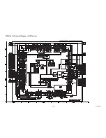
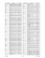
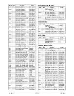
IC612 ( FIP DRIVER )
97
-
CTL
To Monitor for
CTL AMP Output
PULSE
98
-
AMPVcc AMPVcc
-
99
-
AVcc
A/D Converter
Power Input/
Standard Voltage
Input
-
100
IN
AGC
IF AGC
Comparator
Signal
A/D
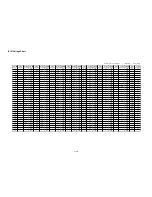
Pin
No.
IN/
OUT
Signal
Name
Name Function
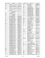
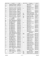
1 IN FP-CLK
Clock Input
2 IN FP-STB
Serial Interface Strobe
3 -
NU
Not Used
4 -
NU
Not Used
5 - VSS GND
6 - VDD
Power Supply
7
OUT
a
Segment Output
8 b
9 c
10 d
11 e
12 f
13 g
14 h
15 - VEE Pull Down Level
16 OUT
i
Segment Output
17
OUT
7G
Grid Output
18
6G
19
5G
20 4G
21 3G
22 2G
23 1G
24 - VDD Power Supply
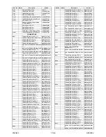
Pin
No.
Mark
IN/
OUT
Signal
Name
Function
Active
Level
25 - VSS GND
26 IN OSC Oscillator Input
27 -
NU
Not Used
28 IN FP-DIN
Serial Data Input
Pin
No.
IN/
OUT
Signal
Name
Name Function
Summary of Contents for DDVR-6830
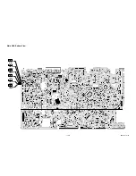
Page 36: ...1 12 6 H9903SCM4 Main 4 8 Schematic Diagram VCR Section...
Page 37: ...1 12 7 H9903SCM5 Main 5 8 Schematic Diagram VCR Section...
Page 38: ...1 12 8 H9903SCM6 Main 6 8 Schematic Diagram VCR Section...
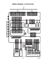
Page 40: ...1 12 10 H9903CM8 Main 8 8 Schematic Diagram VCR Section...
Page 42: ...1 12 12 H9903SCJ Jack A Schematic Diagram VCR Section...
Page 43: ...1 12 13 H9903SCAFV AFV Schematic Diagram VCR Section...
Page 45: ...1 12 15 H9903SCD2 DVD Main 2 3 Schematic Diagram DVD Section...
Page 47: ...1 12 17 H9903SCD3 DVD Main 3 3 Schematic Diagram DVD Section...


