background image

SERVICE MANUAL

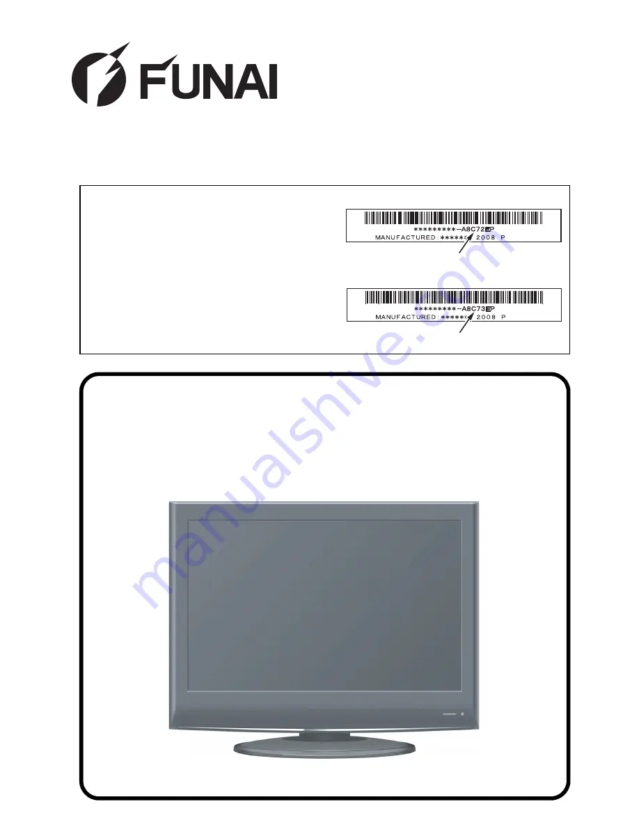
This Service Manual is for the 
LT6-M22BB(A8C72EP)
/LT6-M22WB(A8C73EP) model.
For the LT6-M22BB(A8C72EP)
/LT6-M22WB(A8C73EP) model, 
the letter (A8C72EP)/(A8C73EP) is 
printed on the Serial No. Label. 
Refer to the Serial No. Label on the 
right.

Serial No. Label

"A8C72EP"

Serial No. Label

"A8C73EP"

22

 COLOR LCD TELEVISION

LT6-M22BB/LT6-M22WB

Summary of Contents for A8C72EP

Page 1: ...T6 M22WB A8C73EP model For the LT6 M22BB A8C72EP LT6 M22WB A8C73EP model the letter A8C72EP A8C73EP is printed on the Serial No Label Refer to the Serial No Label on the right Serial No Label A8C72EP Serial No Label A8C73EP 22 COLOR LCD TELEVISION LT6 M22BB LT6 M22WB ...

Page 2: ...tions 5 1 How to Initialize the LCD Television 6 1 Block Diagrams 7 1 Schematic Diagrams CBA and Test Points 8 1 Waveforms 9 1 Wiring Diagram 10 1 Exploded View 11 1 Mechanical Parts List 12 1 Electrical Parts List 13 1 The LCD panel is manufactured to provide many years of useful life Occasionally a few non active pixels may appear as a tiny spec of color This is not to be considered a defect in ...

Page 3: ...0 to 80 Description Condition Unit Nominal Limit 1 RECEIVED FREQ RANGE 60dBm 45ch 1 kHz kHz 1000 900 500 150 2 INPUT DYNAMIC RANGE mix max 1 VHF HIGH 7ch UHF 45ch dBm dBm 82 5 2 81 1 2 75 10 75 10 3 C N PERFORMANCE 1 VHF HIGH 7ch UHF 45ch dB dB 15 15 18 18 4 MULTIPATH a Performance with short delay echoes b Performance with long delay echoes c C N Performance on 0dB echo channel 14µs UHF 45ch c 2 ...

Page 4: ...elow these specifications Limit specifications represent the absolute worst condition that still might be considered acceptable In no case should a unit fail to meet limit specifications Description Condition Unit Nominal Limit 1 Audio Output Power 10 THD Lch Rch W 1 0 1 0 0 8 0 8 2 Audio Distortion 500mW Lch Rch 1 5 1 5 3 0 3 0 3 Audio Freq Response 6dB Lch 6dB Rch Hz Hz 70 to 8 k 70 to 8 k 4 Aud...

Page 5: ...d terminal screw and if applicable to the coaxial connector If the measured resistance is less than 1 0 megohm or greater than 5 2 megohm an abnormality exists that must be corrected before the instrument is returned to the customer Repeat this test with the instrument AC switch in the off position d Leakage Current Hot Check With the instrument completely reassembled plug the AC line cord directl...

Page 6: ...b near thermally hot parts be sure that leads and components do not touch thermally hot parts c the AC supply d high voltage and e antenna wiring Always inspect in all areas for pinched out of place or frayed wiring Check AC power cord for damage 6 Components parts and or wiring that appear to have overheated or are otherwise damaged should be replaced with components parts or wiring that meet ori...

Page 7: ... PVC tubing 3 Spacers 4 Insulators for transistors E When replacing AC primary side components transformers power cord etc wrap ends of wires securely about the terminals before soldering F Observe that the wires do not contact heat producing parts heat sinks oxide metal film resistors fusible resistors etc G Check that replaced wires do not contact sharp edged or pointed parts H When a power cord...

Page 8: ... and externally exposed accessible parts RF terminals an tenna terminals video and audio input and output ter minals microphone jacks earphone jacks etc Measuring Method Power ON Insert load Z between B earth ground power cord plug prongs and exposed accessible parts Use an AC voltmeter to measure across both terminals of load Z See Fig 2 and following table Table 2 Leakage current ratings for sel...

Page 9: ...f the flat pack IC is fixed with glue to the CBA when removing entire flat pack IC first apply soldering iron to center of the flat pack IC and heat up Then remove glue will be melted Fig S 1 6 4 Release the flat pack IC from the CBA using tweezers Fig S 1 6 CAUTION 1 The Flat Pack IC shape may differ by models Use an appropriate hot air flat pack IC desoldering machine whose shape matches that of...

Page 10: ...pins of the flat pack IC you can remove it easily Fig S 1 3 2 Affix the wire to a workbench or solid mounting point as shown in Fig S 1 5 3 While heating the pins using a fine tip soldering iron or hot air blower pull up the wire as the solder melts so as to lift the IC leads from the CBA contact pads as shown in Fig S 1 5 4 Bottom of the flat pack IC is fixed with glue to the CBA when removing en...

Page 11: ...r due to a potential difference caused by electrostatic charge during unpacking or repair work 1 Ground for Human Body Be sure to wear a grounding band 1 MΩ that is properly grounded to remove any static electricity that may be charged on the body 2 Ground for Workbench Be sure to place a conductive sheet or copper plate with proper grounding 1 MΩ on the workbench or other surface where the semi c...

Page 12: ...in the Table Step Loc No Part Removal Fig No Remove Unhook Unlock Release Unplug Unclamp Desolder Note 1 Stand Cover D1 2 S 1 2 Neck Cover D1 3 Rear Cabinet D1 2 S 2 3 S 3 12 S 4 4 Stand Hinge D1 5 Jack CBA D2 D3 2 S 5 CN107 7 Digital Main CBA Unit 5 Jack CBA 13 IR Sensor CBA 1 Stand Cover 2 Neck Cover 3 Rear Cabinet 14 Function CBA 16 Speaker s 4 Stand Hinge 6 Shield Box 17 Front Cabinet 10 Main ...

Page 13: ...4 2 A8C72DC 3 Rear Cabinet S 1 S 4 S 2 S 3 S 3 S 3 S 4 S 4 S 4 S 4 S 4 1 Stand Cover 2 Neck Cover 4 Stand Hinge Fig D1 ...

Page 14: ... 9 S 10 5 Jack CBA 13 IR Sensor CBA 6 Shield Box 8 FFC Shield 9 Shield T 11 Junction CBA 12 Inverter CBA 17 Front Cabinet 10 Main CBA 14 Function CBA 16 Speaker 7 Digital Main CBA Unit 15 LCD Module Assembly 16 Speaker Connector IC Card OSU Speaker Holders Speaker Holders S 18 S 13 Fig D2 ...

Page 15: ...Main CBA CN802 CN202 CN4501 CN4502 CN11 Digital Main CBA Unit Jack CBA CN201 CN3704 CN4503 CN3701 CN3601 CN103A CN102A CN101A CN104A To LCD Module Assembly CN107 To Speaker Fig D3 CN403 CN402 CN451 CN401 To Speaker Junction CBA Inverter CBA To LCD Module Assembly CN404B CN404A CL404 ...

Page 16: ...nts have been completed Also do not attempt these adjustments unless the proper equipment is available Test Equipment Required 1 DC Voltmeter 2 Pattern Generato 3 Color Analyzer How to make the Service remote control unit Cut A portion of the attached remote control unit as shown in Fig 1 How to set up the service mode Service mode 1 Use the service remote control unit 2 Turn the power on 3 Press ...

Page 17: ... The optical receptor must be set perpendicularly to the LCD Panel surface 3 Enter the Service mode 4 VCOM1 Press 2 button on the service remote control unit VCOM2 Press 3 button on the service remote control unit 5 Press P buttons on the service remote control unit so that the color analyzer value becomes minimum 7 button Note When entering this mode the default setting is White mode Purity Check...

Page 18: ... the LCD Panel surface 4 Enter the Service mode Press button on the service remote control unit and select C D mode 5 CUTOFF Press 3 button to select COB for Blue Cutoff adjustment Press 1 button to select COR for Red Cutoff adjustment DRIVE Press 6 button to select DB for Blue Drive adjustment Press 4 button to select DR for Red Drive adjustment 6 In each color mode press P buttons to adjust the ...

Page 19: ...ice button on the service remote control unit Refer to page 5 1 To cancel the service mode Press button on the remote control unit 3 Press button on the service remote control unit to initialize the LCD television 4 INITIALIZED will appear in the upper right of the screen INITIALIZED color will change to green from red when initializing is complete ...

Page 20: ... N22 AMP MUTE SUB 18 REMOTE R22 RESET MAIN 5 RESET MAIN TO AUDIO 2 BLOCK DIAGRAM V24 LED1 4 4 REMOTE 2 2 P ON H1 5 5 CN201 KEY IN1 6 6 CN106 LED1 18 8 CN101A P ON H2 13 13 CN3701 KEY IN1 25 1 KEY IN1 24 VCOM PWM 21 VCOM PWM AA2 AMP MUTE MAIN AMP MUTE SCL SDA 19 20 IC3102 MEMORY 5 6 SDA SCL PROTECT2 RESET 23 PROTECT1 21 5 CN101A CN3701 PROTECT2 20 6 RESET 17 9 4 PROTECT3 PROTECT3 19 7 IC3706 MEMORY...

Page 21: ...DEO G VIDEO B TO DIGITAL SIGNAL PROCESS BLOCK DIAGRAM S VIDEO Y S VIDEO C TO DIGITAL SIGNAL PROCESS BLOCK DIAGRAM COMP Pb COMP Y COMP Pr TS DATA TO DIGITAL SIGNAL PROCESS BLOCK DIAGRAM 25 26 SCL SDA SCL SDA TO SYSTEM CONTROL BLOCK DIAGRAM AUDIO SIGNAL INPUT2 TO SYSTEM CONTROL BLOCK DIAGRAM MAIN CBA DIGITAL MAIN CBA UNIT 15 11 7 VIDEO B VIDEO G VIDEO R JK721 S VIDEO IN C Y 8 19 20 VIDEO IN VIDEO OU...

Page 22: ...SELECT SW CTL 13 12 15 10 9 11 1 2 14 IC3822 AUDIO D A CONVERTER D A CONVERTER L CH R CH 15 14 5 6 8 7 L CH R CH Q3831 BUFFER Q3832 BUFFER Q3833 Q3834 SCART MUTE CN3704 CN103A SIF 9 15 ADATA1 TO SYSTEM CONTROL BLOCK DIAGRAM MAIN CBA IC850 INPUT SELECT SW CTL 13 1 2 4 12 11 9 10 L CH R CH AUDIO L IN JK723 JK724 AUDIO R IN 3 15 JK751 3 1 AUDIO L OUT AUDIO R OUT 6 AUDIO L IN 2 AUDIO R IN IC851 INPUT ...

Page 23: ...ND 2 SP802 SPEAKER L CH CN802 CL802 SP L 1 SP GND 2 MAIN CBA MUTE STANDBY CONTROL IC802 AUDIO D A CONVERTER D A CONVERTER L CH R CH 15 14 5 6 7 8 ACLK 14 12 ADATA 13 13 BCLK 12 14 LRCLK 11 15 CN101A CN3701 AMP MUTE 9 17 ACLK BCLK LRCLK ADATA TO DIGITAL SIGNAL PROCESS BLOCK DIAGRAM AMP MUTE TO SYSTEM CONTROL BLOCK DIAGRAM JUNCTION CBA SP R 13 13 SP R 13 13 CN404A CN105A CN404B CL404 INVERTER CBA Q8...

Page 24: ... MEMORY 5 6 SDA SCL D SUB 3 12 15 1 2 RED GREEN BLUE DATA CLOCK JK3701 T5 R4 R3 R5 A D CONVERTER 14 13 HSYNC VSYNC K5 L5 COMP Pr VIDEO S VIDEO Y S VIDEO C VIDEO R VIDEO G VIDEO B TO VIDEO BLOCK DIAGRAM SW W3 U3 V3 V4 Y2 Y1 AA1 COMP Pb T3 COMP Y U4 T4 TU CVBS Y3 VGA HSYNC VGA VSYNC HDMI IN1 JK4001 TMDS D0 TMDS D0 TMDS D1 TMDS D1 TMDS D2 TMDS D2 SDA SCL 7 9 4 6 1 3 10 12 16 15 A9 B9 C8 C9 B8 A8 B10 ...

Page 25: ...TCHING OSC PWM CONTROL LOGIC VCC CURRENT CONTROL SWITCH CURRENT CONTROL SWITCH OVER VOLTAGE PROTECTOR OVER VOLTAGE PROTECTOR OVER VOLTAGE PROTECTOR OVER VOLTAGE PROTECTOR OVER VOLTAGE PROTECTOR OVER VOLTAGE PROTECTOR 8 11 5 6 15 3 12 16 2 1 SW 22V SW SW 16V Q428 CN404B TO SYSTEM CONTROL BLOCK DIAGRAM CN105A CN404B INVERTER CBA LCD MODULE ASSEMBLY TO POWER SUPPLY BLOCK DIAGRAM CN105A JUNCTION CBA C...

Page 26: ... 23 P ON 5V 1 2 24 25 LCD 3 3V 12 14 P ON 9V 14 12 LCD 6 8V 10 16 LCD 13V 5 7 19 21 P ON 3 3V 15 17 9 11 Q908 SW 6 8V IC902 3 3V REG 1 2 4 LCD 24 5V LCD 6 8V LCD 13V P ON 3 3V 3 5V 1 3 5V 2 LCD 3 3V AL 3 3V P ON 5V P ON 9V DIGITAL MAIN CBA UNIT TO INVERTER BLOCK DIAGRAM CL404 3 5V 1 18 19 7 8 3 5V 2 22 24 2 4 NOTE The voltage for parts in hot circuit is measured using hot GND as a common terminal ...

Page 27: ...in the schematic diagram and the parts list Before replacing any of these components read the parts list in this manual carefully The use of substitute replacement parts that do not have the same safety characteristics as specified in the parts list may create shock fire or other hazards Notes 1 Do not use the part number shown on these drawings for ordering The correct part number is shown in the...

Page 28: ...ed 2 To maintain original function and reliability of repaired units use only original replacement parts which are listed with their part numbers in the parts list section of the service manual 4 Voltage indications on the schematics are as shown below Plug the TV power cord into a standard AC outlet 5 How to read converged lines 6 Test Point Information 2 3 1 5 0 5 0 Voltage Indicates that the vo...

Page 29: ...8 3 A8C72SCM1 Main 1 3 Schematic Diagram ...

Page 30: ...8 4 A8C72SCM2 Main 2 3 Jack Schematic Diagram ...

Page 31: ...that all components in the power supply circuit are not defective before you connect the AC plug to the AC power supply Otherwise it may cause some components in the power supply circuit to fail CAUTION For continued protection against fire hazard replace only with the same type fuse NOTE The voltage for parts in hot circuit is measured using hot GND as a common terminal ...

Page 32: ...8 6 A8C72SCINV Inverter Junction Schematic Diagram ...

Page 33: ...8 7 Function Schematic Diagram A8C72SCF ...

Page 34: ...8 8 IR Sensor Schematic Diagram A8C72SCIR ...

Page 35: ...Main 1 6 Schematic Diagram The order of pins shown in this diagram is different from that of actual IC4513 IC4513 is divided into seven and shown as IC4513 1 5 IC4513 4 5 in this Digital Main Schematic Diagram Section 1 NOTE ...

Page 36: ...Main 2 6 Schematic Diagram The order of pins shown in this diagram is different from that of actual IC4513 IC4513 is divided into seven and shown as IC4513 1 5 IC4513 4 5 in this Digital Main Schematic Diagram Section 1 NOTE ...

Page 37: ...Main 3 6 Schematic Diagram The order of pins shown in this diagram is different from that of actual IC4513 IC4513 is divided into seven and shown as IC4513 1 5 IC4513 4 5 in this Digital Main Schematic Diagram Section 1 NOTE ...

Page 38: ...Main 4 6 Schematic Diagram The order of pins shown in this diagram is different from that of actual IC4513 IC4513 is divided into seven and shown as IC4513 1 5 IC4513 4 5 in this Digital Main Schematic Diagram Section 1 NOTE ...

Page 39: ...8 13 A8C72SCD5 Digital Main 5 6 Schematic Diagram ...

Page 40: ...Main 6 6 Schematic Diagram The order of pins shown in this diagram is different from that of actual IC4513 IC4513 is divided into seven and shown as IC4513 1 5 IC4513 4 5 in this Digital Main Schematic Diagram Section 1 NOTE ...

Page 41: ...unit If Main Fuse F601 is blown check to see that all components in the power supply circuit are not defective before you connect the AC plug to the AC power supply Otherwise it may cause some components in the power supply circuit to fail Because a hot chassis ground is present in the power supply circut an isolation transformer must be used Also in order to have the ability to increase the input...

Page 42: ...tage or Auto voltage selectable power supply circuit is used in this unit If Main Fuse F601 is blown check to see that all components in the power supply circuit are not defective before you connect the AC plug to the AC power supply Otherwise it may cause some components in the power supply circuit to fail Because a hot chassis ground is present in the power supply circut an isolation transformer...

Page 43: ...8 17 BA8A70F01021 1 Inverter CBA Top View ...

Page 44: ...8 18 BA8A70F01021 1 Inverter CBA Bottom View ...

Page 45: ...8 19 IR Sensor CBA Top View Function CBA Top View Function CBA Bottom View BA8C72F01012 2 BA8C72F01012 3 IR Sensor CBA Bottom View ...

Page 46: ...8 20 Jack CBA Top View Jack CBA Bottom View BA8C72F01012 4 Junction CBA Top Bottom View BA8A70F01021 ...

Page 47: ...Shown in Schematic Diagram WF1 Pin 14 of IC801 AUDIO 0 1V 0 5ms WF2 Pin 23 of CN101A S VIDEO Y 0 2V 10µs WF3 Pin 25 of CN101A S VIDEO C 0 2V 20µs WF4 Pin 5 of CN102A B 0 5V 5µs WF7 Pin 1 of CN102A WF5 Pin 4 of CN102A G 0 5V 20µs VIDEO 0 2V 20µs WF6 Pin 3 of CN102A R 0 5V 10µs VIDEO B 0 5V 20µs VIDEO G 0 5V 20µs VIDEO R 0 5V 20µs ...

Page 48: ... L SP GND SP802 SPEAKER L CH JACK CBA CN201 CN106 1 3 2 4 5 GND REMOTE AL 3 3V P ON H1 6 KEY IN1 LED1 6 2 4 5 3 1 CN301 CN202 1 3 2 4 5 GND REMOTE AL 3 3V P ON H1 LED1 2 4 5 3 1 CN451 BACK LIGHT CN402 BACK LIGHT CN401 2 1 BACK LIGHT CN403 2 1 2 1 2 1 AC601 AC CORD 30 GMA7 GMA6 GMA5 GMA4 GMA3 29 28 27 26 25 GMA2 GMA1 GND 24 23 22 BRSCLK 21 BRSCLK 20 GND 19 TP1 18 POL 17 BRSR2 16 BRSR2 15 BRSR1 46 B...

Page 49: ...1 CL4503 CL3701 CL3704 CN3802 L29 L36 B36 L10 L10 L28 L10 B36 Digital Main CBA Unit A5 B32 A1 A11 A7 L30 L30 B47 L30 L30 SP451 CL451 SP802 Function CBA IR Sensor CBA B1 B1 B1 B1 CL802 B47 L30 LCD1 L10 B43 L10 Inverter CBA Junction CBA L17 L9 L9 L9 B22 AC601 B41 B42 L30 L32 B43 L32 CL4502 CL4501 L10 L10 L4 B9 B29 L10 A24 B15 A9 L11 L2 L10 B10 L10 L10 Jack CBA A21 Main CBA B35 ...

Page 50: ...NT FRONT S2 S4 Tape Packing Tape S3 S3 X1 Some Ref Numbers are not in sequence X4 X3 Packing Tape Packing Tape Packing Tape S6 S5 X2 1 X2 2 X2 3 Owners Manual AR Owners Manual BG Owners Manual EN Owners Manual RU Owners Manual UA ...

Page 51: ...FFC WIRE 55PIN 42MM WX1A8A70 101 CL4502 WIRE ASSEMBLY FFC 55PIN FFC WIRE 55PIN 42MM WX1A8A70 101 CL4503 FFC WIRE 25PIN WX1A8C70 005 WX1A8C70 005 CN3802 CONNECTOR IC CARD OSU SLOT 2013858 1 J620680AP001 L2 SCREW P TIGHT M3X8 BIND HEAD GBJP3080 L10 SCREW S TIGHT M3X6 BIND HEAD GBJS3060 L17 DOUBLE SEMS SCREW M4X9 BLACK L0130UA 0EM408146A L28 HEX SCREW 4 40 7MM 1EM422042 L29 DOUBLE SEMS SCREW M2X10 M2...

Page 52: ... FREE 0 01µF 100V J or CA2A103DT018 CAP POLYESTER FILM 0 01µF 100V J CA2A103SER02 C624 POLYESTER FILM CAP PB FREE 0 0015µF 100V J or CA2A152DT018 CAP POLYESTER FILM 0 0015µF 100V J CA2A152SER02 C625 POLYESTER FILM CAP PB FREE 0 068µF 100V J or CA2A683DT018 CAP POLYESTER FILM 0 068µF 100V J CA2A683SER02 C630 SAFTY CAP 1000pF 250V KX or CA2E102MR101 SAFETY CAP 1000pF 250V KX or CA2E102MR050 CAP CERA...

Page 53: ...D1JZ30F104 C922 ELECTROLYTIC CAP 10µF 50V M CE1JMASDL100 C923 ELECTROLYTIC CAP 10µF 50V M CE1JMASDL100 C924 ELECTROLYTIC CAP 470µF 16V M CE1CMASDL471 C925 ELECTROLYTIC CAP 10µF 50V M CE1JMASDL100 C926 CHIP CERAMIC CAP 1608 F Z 0 1µF 50V CHD1JZ30F104 Ref No Mark Description Part No C927 ELECTROLYTIC CAP 10µF 50V M CE1JMASDL100 C940 CHIP CERAMIC CAP 1608 F Z 0 1µF 50V CHD1JZ30F104 C941 ELECTROLYTIC ...

Page 54: ...TCHING HSS4148TE E QDTZ0HSS4148 D944 SWITCHING DIODE 1SS133 T 77 or QDTZ001SS133 DIODE SWITCHING HSS4148TE E QDTZ0HSS4148 Ref No Mark Description Part No D947 SWITCHING DIODE 1SS133 T 77 or QDTZ001SS133 DIODE SWITCHING HSS4148TE E QDTZ0HSS4148 D948 SWITCHING DIODE 1SS133 T 77 or QDTZ001SS133 DIODE SWITCHING HSS4148TE E QDTZ0HSS4148 D951 ZENER DIODE MTZJT 7715B QDTB00MTZJ15 D953 SWITCHING DIODE 1SS...

Page 55: ...9P TRANSISTOR KTC3198 GR AT P or NQS4KTC3198P TRANSISTOR 2SC1815 GR TE2 F T or QQS12SC1815F NPN TRANSISTOR 2SC5343G AT or NQSG02SC5343 Ref No Mark Description Part No NPN TRANSISTOR 2SC5343MG AT NQSG2SC5343M Q904 TRANSISTOR KTC3199 GR AT P or NQS4KTC3199P TRANSISTOR KTC3198 GR AT P or NQS4KTC3198P TRANSISTOR 2SC1815 GR TE2 F T or QQS12SC1815F NPN TRANSISTOR 2SC5343G AT or NQSG02SC5343 NPN TRANSIST...

Page 56: ... J 75 Ω RRXA750YF002 R766 CARBON RES 1 4W J 100 Ω RCX4JATZ0101 Ref No Mark Description Part No R767 CHIP RES 1 10W J 1 2k Ω or RRXAJR5Z0122 RES CHIP 1608 1 10W J 1 2k Ω RRXA122YF002 R768 CARBON RES 1 4W J 470 Ω RCX4JATZ0471 R770 CHIP RES 1 10W J 75 Ω or RRXAJR5Z0750 RES CHIP 1608 1 10W J 75 Ω RRXA750YF002 R771 CARBON RES 1 4W J 150 Ω RCX4JATZ0151 R775 CHIP RES 1 10W J 10k Ω or RRXAJR5Z0103 RES CHI...

Page 57: ...ES 1 10W F 4 7k Ω or RRXAFR5Z0472 RES CHIP 1608 1 10W F 4 70k Ω RTW4701YF002 Ref No Mark Description Part No R908 CHIP RES 1 10W F 3 9k Ω or RRXAFR5H3901 CHIP RES 1608 1 10W F 3 9k Ω or RRXAFR5Z3901 RES CHIP 1608 1 10W F 3 90k Ω RTW3901YF002 R909 CHIP RES 1 10W F 3 9k Ω or RRXAFR5H3901 CHIP RES 1608 1 10W F 3 9k Ω or RRXAFR5Z3901 RES CHIP 1608 1 10W F 3 90k Ω RTW3901YF002 R910 CHIP RES 1 10W F 820...

Page 58: ...RRXAJR5Z0682 RES CHIP 1608 1 10W J 6 8k Ω RRXA682YF002 R985 CARBON RES 1 4W J 2 7k Ω RCX4JATZ0272 R986 CHIP RES 1 10W F 240 Ω or RRXAFR5H2400 CHIP RES 1608 1 10W F 240 Ω or RRXAFR5Z2400 RES CHIP 1608 1 10W F 240 Ω RTW2400YF002 R987 CHIP RES 1 10W J 100 Ω or RRXAJR5Z0101 RES CHIP 1608 1 10W J 100 Ω RRXA101YF002 Ref No Mark Description Part No R992 PCB JUMPER D0 6 P5 0 JW5 0T R994 CHIP RES 1 10W F 3...

Page 59: ... or RRXAJR5Z0331 RES CHIP 1608 1 10W J 330 Ω RRXA331YF002 R304 CHIP RES 1 10W J 3 3k Ω or RRXAJR5Z0332 RES CHIP 1608 1 10W J 3 3k Ω RRXA332YF002 MISCELLANEOUS RS301 SENSOR REMOTE RECEIVER KSM 712TH2E USESJRSKK044 Ref No Mark Description Part No Ref No Mark Description Part No JACK CBA Consists of the following CAPACITORS C14 CHIP CERAMIC CAP 1608 B K 5600pF 50V CHD1JK30B562 C15 CHIP CERAMIC CAP 16...

Page 60: ...K 0 022µF 50V CHD1JK30B223 C467 CHIP CERAMIC CAP 1608 B K 0 022µF 50V CHD1JK30B223 C468 CHIP CERAMIC CAP 1608 B K 0 022µF 50V CHD1JK30B223 C469 CHIP CERAMIC CAP 1608 B K 0 022µF 50V CHD1JK30B223 C470 CHIP CERAMIC CAP 1608 B K 0 022µF 50V CHD1JK30B223 Ref No Description Part No C481 CHIP CERAMIC CAP 1608 CH J 1000pF 50V CHD1JJ3CH102 C482 CHIP CERAMIC CAP 1608 C0G J 220pF 100V CA2A221MR133 C483 CHIP...

Page 61: ...STOR 2SC1815 GR TE2 F T or QQS12SC1815F Ref No Description Part No NPN TRANSISTOR 2SC5343MG AT NQSG2SC5343M Q409 TRANSISTOR KTC3199 GR AT P or NQS4KTC3199P TRANSISTOR KTC3198 GR AT P or NQS4KTC3198P TRANSISTOR 2SC1815 GR TE2 F T or QQS12SC1815F NPN TRANSISTOR 2SC5343MG AT NQSG2SC5343M Q410 TRANSISTOR 2SC2120 Y TE2 F T or QQSY2SC2120F TRANSISTOR 2SC2120 O TE2 F T or QQS02SC2120F TRANSISTOR KTC3203 ...

Page 62: ...50 CHIP RES 1 10W J 390 Ω or RRXAJR5Z0391 RES CHIP 1608 1 10W J 390 Ω RRXA391YF002 Ref No Description Part No R451 CHIP RES 1 10W J 10k Ω or RRXAJR5Z0103 RES CHIP 1608 1 10W J 10k Ω RRXA103YF002 R452 CHIP RES 1 10W J 10k Ω or RRXAJR5Z0103 RES CHIP 1608 1 10W J 10k Ω RRXA103YF002 R453 CHIP RES 1 10W J 3 3k Ω or RRXAJR5Z0332 RES CHIP 1608 1 10W J 3 3k Ω RRXA332YF002 R454 CHIP RES 1 10W J 10 Ω or RRX...

Page 63: ... 1 10W J 12k Ω or RRXAJR5Z0123 RES CHIP 1608 1 10W J 12k Ω RRXA123YF002 R504 CHIP RES 1 10W J 47k Ω or RRXAJR5Z0473 RES CHIP 1608 1 10W J 47k Ω RRXA473YF002 R506 CHIP RES 1 10W J 10k Ω or RRXAJR5Z0103 RES CHIP 1608 1 10W J 10k Ω RRXA103YF002 R507 CHIP RES 1 10W J 1k Ω or RRXAJR5Z0102 RES CHIP 1608 1 10W J 1 0k Ω RRXA102YF002 R508 CHIP RES 1 10W J 1k Ω or RRXAJR5Z0102 RES CHIP 1608 1 10W J 1 0k Ω R...

Page 64: ...LT6 M22BB LT6 M22WB A8C72 73EP 2008 11 26 ...

Reviews: