


324
CHAPTER 15 UART
15.6 Receive-Interrupt Generation and Flag Set Timing
The receive interrupts are interrupts indicating receive completion (SSR0-3: RDRF)
and receive-error generation (SSR0-3: PE, ORE, FRE).
■
Receive-interrupt generation and flag set timing
When the stop bit is detected (in operation modes 0 to 4) or when the final bit (D7) of the data is
detected (in operation mode 2) during reception, the receive data is stored in input-data register
1 (SIDR0-3). In case of a receive error, the error flag (SSR0-3: PE, ORE, FRE) is set. After this,
the receive data full flag (SSR0-3: RDRF) is set to 1. In each mode, the SIDR0-3 value is invalid
when the error flag is 1.
❍
Operation mode 0 (asynchronous, normal mode)
When the stop bit is detected, the RDRF is set to 1. When a receive error occurs, the error flag
(PE, ORE, FRE) is set.
❍
Operation mode 1 (asynchronous, multiprocessor mode)
When the stop bit is detected, the RDRF is set to 1. When a receive error occurs, the error flag
(ORE, FRE) is set. Parity errors cannot be detected.
❍
Operation mode 2 (synchronous, normal mode)
When the final bit (D7) of receive data is detected, the RDRF is set to 1. If a receive error
occurs, the error flag (ORE) is set. Parity errors and framing errors cannot be detected. Figure
15.6-1 "Receive operation and flag set timing" shows the receive operation and flag set timing.
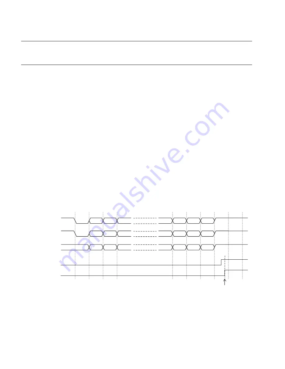
Figure 15.6-1 Receive operation and flag set timing
❍
Timing of receive-interrupt generation
A receive-interrupt request is issued immediately after the RDRF, PE, ORE, or FRE flag is set to
1 while receive interrupts are enabled (SSR0-3: RIE = 1).
ST
D0
SP
D1
D5
D6
D7/P
ST
D0
SP
D1
D6
D7
A/D
PE, ORE, FRE*
RDRF
Receive-interrupt generation
D0
D7
D1
D4
D5
D6
*: The PE flag cannot be used in mode 1.
The PE and FRE flags cannot be used in mode 2.
ST: Start bit
SP: Stop bit
A/D: Mode 2 (multiprocessor mode) address/data selection bit
Receive data
(Operation mode 0)
Receive data
(Operation mode 1)
Receive data
(Operation mode 2)
Summary of Contents for MB91150 Series
Page 1: ......
Page 2: ......
Page 3: ...FUJITSU LIMITED FR30 32 BIT MICROCONTROLLER MB91150 Series HARDWARE MANUAL ...
Page 4: ......
Page 10: ...vi ...
Page 112: ...96 CHAPTER 3 MEMORY SPACE CPU AND CONTROL UNIT ...
Page 178: ...162 CHAPTER 5 I O PORTS ...
Page 214: ...198 CHAPTER 7 16 BIT RELOAD TIMER ...
Page 240: ...224 CHAPTER 8 PPG TIMER ...
Page 310: ...294 CHAPTER 13 8 10 BIT A D CONVERTER ...
Page 318: ...302 CHAPTER 14 8 BIT D A CONVERTER ...
Page 362: ...346 CHAPTER 15 UART ...
Page 420: ...404 CHAPTER 19 PERIPHERAL STOP CONTROL ...
Page 428: ...412 CHAPTER 20 CALENDAR MACROS ...
Page 503: ...487 INDEX INDEX The index follows on the next page This is listed in alphabetic order ...
Page 510: ...494 INDEX ...
Page 512: ......