


MPC563XM Reference Manual, Rev. 1
398
Freescale Semiconductor
Preliminary—Subject to Change Without Notice
13.6.3
Running with Asynchronous Memories
The EBI also supports asychronous memories. In this case, the CLKOUT, TS, and BDIP pins are not used
by the memory and bursting is not supported. However, the EBI still drives these outputs, and always
drives and latches all signals at posedge CLKOUT (i.e., there is no "asynchronous mode" for the EBI). The
data timing is controlled by setting the SCY bits in the appropriate Option Register to the proper number
of wait states to work with the access time of the asynchronous memory, just as done for a synchronous
memory.
13.6.3.1
Example Wait State Calculation
This example applies to any chip-select memory, synchronous or asynchronous.
As an example, say we have a memory with 50ns access time, and we are running the external bus
@ 66 MHz (CLKOUT period: 15.2ns). Assume the input data spec for the MCU is 4ns.
number of wait states = (access time) / (CLKOUT period) + (0 or 1) (depending on setup time)
50/15.2 = 3 with 4.4ns remaining (so we need at least 3 wait states, now check setup time)
15.2-4.4=10.8ns (this is the achieved input data setup time)
Since actual input setup (10.8ns) is greater than the input setup spec (4.0ns), 3 wait states is sufficient. If
the actual input setup was less than 4.0ns, we would have to use 4 wait states instead.
13.6.3.2
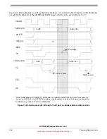
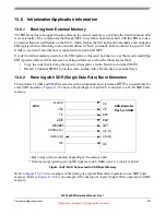
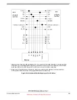
Timing and Connections for Asynchronous Memories
The connections to an asynchronous memory are the same as for a synchronous memory, except that the
CLKOUT, TS, and BDIP signals are not used.
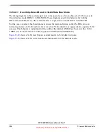
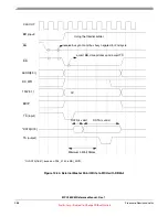
shows a block diagram of an MCU connected
to an asynchronous memory.
Figure 13-54. MCU Connected to Asynchronous Memory
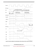
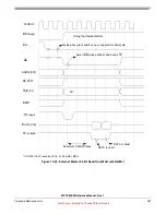
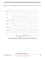
shows a timing diagram of a read operation to a 16-bit asynchronous memory using 3 wait
states.
ADDR[9:30]
A[0:21]
Asynchronous
CE
CS0
Memory
DATA[0:15]
D[0:15]
WE*
OE
OE
MCU
WE0/BE0
* Flash memories typically use one WE signal as shown, RAMs use 2 or 4 (16-bit or 32-bit)