


MPC563XM Reference Manual, Rev. 1
350
Freescale Semiconductor
Preliminary—Subject to Change Without Notice
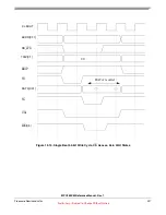
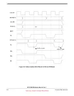
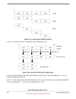
Figure 13-24. Burst 32-bit Read Cycle, One Initial Wait State
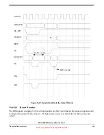
13.5.2.5.1
TBDIP Effect on Burst Transfer
Some memories require different timing on the BDIP signal than the default to run burst cycles. Using the
default value of TBDIP=0 in the appropriate EBI Base Register results in BDIP being asserted (SCY+1)
cycles after the address transfer phase, and being held asserted throughout the cycle regardless of the wait
states between beats (BSCY).
shows an example of the TBDIP=0 timing for a 4-beat burst
with BSCY=1.
CLKOUT
ADDR[3:31]
TS
DATA[0:31]
TA
RD_WR
TSIZ[0:1]
BDIP
‘00’
ADDR[29:31] = ‘000’
Expects another data
Wait State
CSx
OE
DATA is valid


