


MPC563XM Reference Manual, Rev. 1
Freescale Semiconductor
245
Preliminary—Subject to Change Without Notice
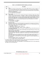
•
Erase suspend, program suspend, and erase-suspended program
•
Shadow information stored in a non-volatile shadow block
•
Independent program/erase of the shadow block
11.5
Modes of Operation
11.5.1
User Mode
User mode is the default operating mode of the Flash memory block. In this mode, you can read, write,
program, and erase the Flash.
11.5.2
Stop Mode
In stop mode (CFLASH_MCR[STOP] = 1), all DC current sources in the Flash are disabled.
11.6
Memory Map/Register Description
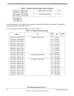
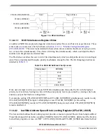
The Flash BIU occupies a 512-MB portion of the address space. The actual Flash array is multiply-mapped
within this space.
11.6.1
Flash Memory Map
shows the Flash array memory map and how it is mapped using byte addressing.
Base addresses for the device are the following:
•
Shadow base address = 0x0020_0000
•
Array base address = 0x0000_0000
•
Test Flash base address = 0x0040_0000
•
Control registers base address = 0xC3F8_8000
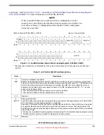
Table 11-1. Module Flash Array Memory Map
Byte Address
Type and Amount of Space Used
Access
Array Base + 0x0000_0000 –
Array Base + 0x0003_FFFF
Low address space (256 KB)
User
Array Base + 0x0004_0000 –
Array Base + 0x0007_FFFF
Mid address space (256 KB)
User
Array Base + 0x0008_0000 –
Array Base + 0x0017_FFFF
High address space (1024 KB)
1
User
Array Base + 0x0008_0000 –
Array Base + 0x000F_FFFF
High address space (512 KB)
2
Array Base + 0x0008_0000 –
Array Base + 0x000B_FFFF
High address space (256 KB)
3


