


MPC563XM Reference Manual, Rev. 1
1216
Freescale Semiconductor
Preliminary—Subject to Change Without Notice
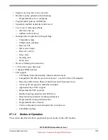
27.1.6.1
Disabled Mode
The Module Disable Bit MDIS in the SCI Control Register 3 can be used to turn off the eSCI. This will
prevent the eSCI core to be clocked, and thus save power.
27.1.6.2
Run Mode
In this mode, the eSCI is fully operational. The eSCI has two major run modes, the SCI mode and the LIN
mode. The availability of certain register bits and fields depends on the selected major run mode.
27.2
External Signal Description
The eSCI module is connected two a total of two external pins.
27.2.1
Detailed Signal Descriptions
27.2.1.1
eSCI Transmit Pin (TXD)
This pin serves as transmit data output and as the receive data input of eSCI.
27.2.1.2
eSCI Receive Pin (RXD)
This pin serves as receive data input of the eSCI.
27.3
Memory Map and Register Definition
This section provides the memory map and a detailed description of the memory mapped registers.
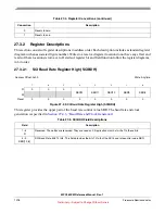
27.3.1
Memory Map
Table 27-3. Block Memory Map
Offset
Register
Access
General Registers
0x00
SCI Baud Rate Register High (SCIBDH)
Read/Write
0x01
SCI Baud Rate Register Low (SCIBDL)
Read/Write
0x02
SCI Control Register 1 (SCICR1)
Read/Write
0x03
SCI Control Register 2 (SCICR2)
Read/Write
0x04
SCI Control Register 3 (SCICR3)
Read/Write
0x05
SCI Control Register 4 (SCICR4)
Read/Write
0x06
SCI Data Register High (SCIDRH)
Read/Write
0x07
SCI Data Register Low (SCIDRL)
Read/Write
0x08
SCI Status Register 1 (SCISR1)
Read/Write


