


MPC563XM Reference Manual, Rev. 1
Freescale Semiconductor
1201
Preliminary—Subject to Change Without Notice
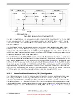
If the CONT bit in the TX FIFO entry is set or the DCONT in the DSPI_DSICR is set, PCS remains
asserted between the transfers. Under certain conditions, SCK can continue with PCS asserted, but with
no data being shifted out of SOUT (SOUT pulled high). This can cause the slave to receive incorrect data.
Those conditions include:
•
Continuous SCK with CONT bit set, but no data in the transmit FIFO.
•
Continuous SCK with CONT bit set and entering STOPPED state (refer to
•
Continuous SCK with CONT bit set and entering Stop mode or Module Disable mode.
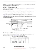
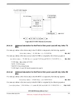
shows timing diagram for Continuous SCK format with Continuous Selection enabled.
Figure 26-37. Continuous SCK Timing Diagram (CONT=1)
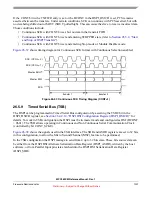
26.5.9
Timed Serial Bus (TSB)
The DSPI can be programmed in Timed Serial Bus configuration by asserting the TSBC bit in the
DSPI_DSICR register, see
Section 26.4.2.10, “DSPI DSI Configuration Register (DSPI_DSICR)
” for
details. To work in TSB configuration the DSPI must be in master mode and configured as DSI (DCONF
= 0b01). The TSB allows operating in Continuous and Non Continuous Serial Communication Clock
(controlled by bit CONT_SCKE).
shows the signals used in the TSB interface. The SDR and ASDR registers are set to 32 bits
in this configuration, to allow the Micro Second Channel (MSC) feature to be performed.
In the TSB configuration the DSPI manage to send from 4 up to 32 bits data. These bits source data can
be either from the DSPI DSI Alternate Serialization Data Register (DSPI_ASDR), written by the host
software, or from Parallel Input pin states latched into the DSPI DSI Serialization Data Register
(DSPI_SDR).
SCK
PCS
SCK
Master SOUT
Master SIN
(CPOL = 0)
(CPOL = 1)
transfer 1
transfer 2


