


MPC563XM Reference Manual, Rev. 1
Freescale Semiconductor
1189
Preliminary—Subject to Change Without Notice
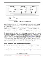
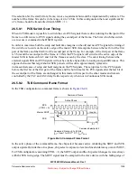
Figure 26-26. CSI Serialization Diagram
The Parallel Inputs signal states are latched into the DSPI DSI Serialization Data Register (DSPI_SDR)
on the rising edge of every system clock and serialized based on the transfer initiation control settings in
the DSPI_DSICR. When SPI frames are written to the TX FIFO they have priority over DSI data from the
DSPI_SDR and are transferred at the next frame boundary. A copy of the most recently transferred DSI
frame is stored in the DSPI_COMPR. The Transfer Priority Logic selects the source of the serialized data
and asserts the appropriate CS signal.
26.5.5.2
CSI Deserialization
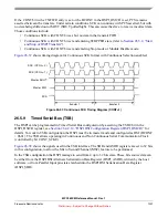
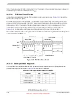
The deserialized frames in CSI Configuration goes into the DSPI_SDR or the RX FIFO based on the
transfer priority logic. When DSI frames are transferred the returned frames are deserialized and latched
into the DSPI_DDR. When SPI frames are transferred the returned frames are deserialized and written to
the RX FIFO.
shows the CSI Deserialization logic.
Figure 26-27. CSI Deserialization Diagram
DSI Control
Clock
Logic
Register
Control
Logic
DSI Transmit
Comparison Register
DSI Serialization
Data Register
16
TX FIFO
Parallel
PCSx (SPI)
SOUT
Shift Register
0 1
15
16
16
16
Logic
Priority
Transfer
PCSy (DSI)
Inputs
SCK
(P_IN)
Slave Bus Interface
DSI Deserialization
Data Register
16
RX FIFO
16
16
Parallel
SIN
Shift Register
0 1
15
Control
Logic
16
Logic
Priority
Transfer
Outputs
(P_OUT)
Slave Bus Interface


