


Chapter 1 Device Overview MC9S12ZVHY/MC9S12ZVHL Families
S12ZVHY/S12ZVHL Family Reference Manual Rev. 1.05
68
Freescale Semiconductor
1.14
The ADC0 VRH/VRL
The ADC0 offers two possible sources for both reference voltages VRH[1:0] and VRL[1:0]. On the
MC9S12ZVHY/MC9S12ZVHL Families only VRH[1], VRL[1] sources are connected at device level(to
VDDA, VSSA respectively), the VRH[0], VRL[0] sources are not connected. Thus the application must
set both VRH_SEL and VRL_SEL in the ADC0CCMD_1 to 1.
1.15
The ADC0 Conversion Resolution
The MC9S12ZVHY/MC9S12ZVHL Families only support 10 and 8 bit converstion resolution, although
ADC block guide still has 12 bit related descrition.
1.16
ADC Result Reference
MCUs of the MC9S12ZVHY/MC9S12ZVHL Families are able to measure the internal reference voltage
V
BG
). V
BG
is a constant voltage with a narrow distribution over temperature and external
A 10-bit right justified
1
ADC conversion result of V
BG
is provided at address 0x1F_C040/0x1F_C041 in
the NVM’s IFR for reference.The measurement conditions of the reference conversion are listed in
Section A.1.10, “ADC Conversion Result Reference”
. By measuring the voltage V
BG
(see
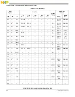
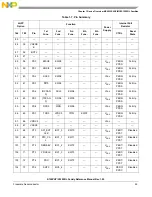
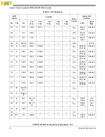
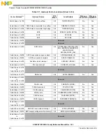
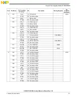
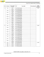
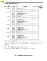
Table 1-14. ADC0 Channel Assignment
ADC0CMD_1 CH_SEL[5:0]
[5]
[4]
[3]
[2]
[1]
[0]
Analog Input
Channel
Usage
0
0
1
0
0
0
Internal_0
ADC temperature sensor
0
0
1
0
0
1
Internal_1
Bandgap Voltage V
BG
or
Vreg temperature sensor
V
HT
0
0
1
0
1
0
Internal_2
RESERVED
0
0
1
0
1
1
Internal_3
RESERVED
0
0
1
1
0
0
Internal_4
V
SENSE
or V
SUP
selectable in BATS
module
0
0
1
1
0
1
Internal_5
RESERVED
0
0
1
1
1
0
Internal_6
RESERVED
0
0
1
1
1
1
Internal_7
RESERVED
1. The format of the stored V
BG
reference value is still subject to change.


