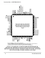

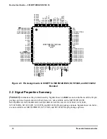


Device User Guide — 9S12DT128DGV2/D V02.16
72
Freescale Semiconductor
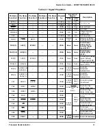
2.3.51 PS5 / MOSI0 — Port S I/O Pin 5
PS5 is a general purpose input or output pin. It can be configured as master output (during master mode)
or slave input pin (during slave mode) MOSI of the Serial Peripheral Interface 0 (SPI0).
2.3.52 PS4 / MISO0 — Port S I/O Pin 4
PS4 is a general purpose input or output pin. It can be configured as master input (during master mode) or
slave output pin (during slave mode) MOSI of the Serial Peripheral Interface 0 (SPI0).
2.3.53 PS3 / TXD1 — Port S I/O Pin 3
PS3 is a general purpose input or output pin. It can be configured as the transmit pin TXD of Serial
Communication Interface 1 (SCI1).
2.3.54 PS2 / RXD1 — Port S I/O Pin 2
PS2 is a general purpose input or output pin. It can be configured as the receive pin RXD of Serial
Communication Interface 1 (SCI1).
2.3.55 PS1 / TXD0 — Port S I/O Pin 1
PS1 is a general purpose input or output pin. It can be configured as the transmit pin TXD of Serial
Communication Interface 0 (SCI0).
2.3.56 PS0 / RXD0 — Port S I/O Pin 0
PS0 is a general purpose input or output pin. It can be configured as the receive pin RXD of Serial
Communication Interface 0 (SCI0).
2.3.57 PT[7:0] / IOC[7:0] — Port T I/O Pins [7:0]
PT7-PT0 are general purpose input or output pins. They can be configured as input capture or output
compare pins IOC7-IOC0 of the Enhanced Capture Timer (ECT).
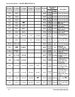
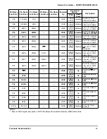
2.4 Power Supply Pins
MC9S12DT128 power and ground pins are described below.
Table 2-2 MC9S12DT128 Power and Ground Connection Summary
Mnemonic
Pin Number
Nominal
Voltage
Description
112-pin QFP
VDD1, 2
13, 65
2.5V
Internal power and ground generated by internal regulator
VSS1, 2
14, 66
0V
Summary of Contents for MC9S12A128
Page 6: ...Device User Guide 9S12DT128DGV2 D V02 16 6 Freescale Semiconductor...
Page 18: ...Device User Guide 9S12DT128DGV2 D V02 16 18 Freescale Semiconductor...
Page 24: ...Device User Guide 9S12DT128DGV2 D V02 16 24 Freescale Semiconductor...
Page 56: ...Device User Guide 9S12DT128DGV2 D V02 16 56 Freescale Semiconductor...
Page 76: ...Device User Guide 9S12DT128DGV2 D V02 16 76 Freescale Semiconductor...
Page 80: ...Device User Guide 9S12DT128DGV2 D V02 16 80 Freescale Semiconductor...
Page 84: ...Device User Guide 9S12DT128DGV2 D V02 16 84 Freescale Semiconductor...
Page 95: ...Device User Guide 9S12DT128DGV2 D V02 16 95 Freescale Semiconductor...
Page 96: ...Device User Guide 9S12DT128DGV2 D V02 16 96 Freescale Semiconductor...
Page 116: ...Device User Guide 9S12DT128DGV2 D V02 16 116 Freescale Semiconductor...
Page 118: ...Device User Guide 9S12DT128DGV2 D V02 16 118 Freescale Semiconductor...
Page 126: ...Device User Guide 9S12DT128DGV2 D V02 16 126 Freescale Semiconductor...
Page 128: ...Device User Guide 9S12DT128DGV2 D V02 16 128 Freescale Semiconductor...
Page 140: ...Device User Guide 9S12DT128DGV2 D V02 16 140 Freescale Semiconductor...
Page 141: ...Device User Guide 9S12DT128DGV2 D V02 16 141 Freescale Semiconductor User Guide End Sheet...


