


FRDM-KL03Z User’s Guide, Rev. 0
8
Freescale Semiconductor
FRDM-KL03Z hardware description
Freescale Semiconductor
8
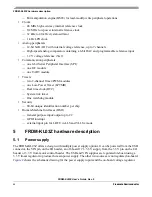
5.4
Serial port
The serial port interface signals used with OpenSDA are UART0 pin PTB1 (TXD) and PTB2 (RXD).
These signals are also connected to I/O header J1.
5.5
Reset
The RESET signal on the KL03Z is connected externally to a push button, SW1. The reset button can be
used to force an external reset event in the target MCU. The reset button can also be used to force the
OpenSDA circuit into bootloader mode when plugging the USB cable to J9. Please refer to
“Serial and Debug Adapter (OpenSDA)
” for more details.
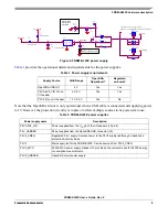
5.6
Debug
The sole debug interface on all Kinetis L Series devices is a Serial Wire Debug (SWD) port. The primary
controller of this interface on the FRDM-KL03Z is the onboard OpenSDA circuit. However, a 2
5-pin
(0.05”) Cortex Debug connector, J7, provides access to the SWD signals for the KL03Z MCU.
shows SWD connector signal descriptions for KL03Z.
5.7
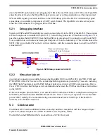
Capacitive touch slider
Two GPIO pins functioning as Touch Sense Input (TSI) signals are connected to capacitive electrodes
configured as a touch slider, as shown in
.
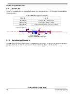
Table 3. ARM JTAG/SWD mini connector description
Pin
Function
Connection to KL03Z
1
VTref
P3V3_MCU
2
SWDIO/TMS
PTA2
3
GND
GND
4
SWDCLK/TCK
PTA0
5
GND
GND
6
SWO/TDO
NC
7
NC
NC
8
TDI
NC
9
NC
NC
10
RESET
PTA1


