background image

5

BOM

Comment

Description

Designator

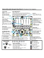
18650 Battery Holder

Battery Charger

BC1

0.1uF

Ceramic Capacitor

C1, C2, C6, C8, C9, C11,C23

220uF

USW0J221MDD1TP

C3, C5

0.047uF

Film Capacitors .047uF 63V 10%

C4

10uF

USW1C100MDD

C7, C20, C21, C22

47uF

USW0J470MDD1TE

C10, C17

3300pf

Film Capacitors 3300 pF 100 VDC 5%

C12

0.1uF

Film Capacitors 0.1uF 63V 5%

C13, C14

680pF

Film Capacitors 680pF 100V 2.5%

C15, C16

10uF

Electrolytic Capacitor 6.3X7mm

C18

0.01uF

Film Capacitors 0.01uF 250 Volts 20%

C19

Header 1X8 M

2.54mm

CN5, CN6

PJ-327U-SMT

3.5mm SMD Headphone Gold Plated

CN?, CN1, CN3, CN4

Led Red 5mm

D1

DC-DC Booster

DC1

Ferrite Bead

FB1

LM386

IC1

PT2399

IC2

ATMEGA328

IC3

10 Ω

Resistor 1/4

R1

5K Ω

Resistor 1/4

R2, R3

Summary of Contents for IC2BS

Page 1: ...1 ...

Page 2: ...able synth was designed to be a new tool in your inventory of sound equipment to help you get started in the world of sound synthesis By reading this manual you ll become familiar with the IC2BS how to use it and how to make the most of it Good luck and have a great experience with your brand new synth from Freedom Enterprise ...

Page 3: ...erface 9 Booting Up 10 Modes Of Operation 11 Monophony And Polyphony 11 Cv And Gate 12 Features And Controls 13 DCO Digitally Controlled Oscillator 13 DCF Digitally Controlled Filter 13 DCA Digitally Controlled Amplifier 14 Modulation 14 Envelope Generator 14 Specifications 17 Creative Commons License 18 Warranty 19 ...

Page 4: ...process Electrostatic discharges or ESD can occur when two electrically charged objects such as the human body and an electronic device come in contact with each other This phenomenon can be of the order of several thousand volts and can destroy integrated circuits like the LM386 PT2399 and ATMEGA328P To prevent this from happening touch a metal surface like a door knob before handling any IC A WA...

Page 5: ... C10 C17 3300pf Film Capacitors 3300 pF 100 VDC 5 C12 0 1uF Film Capacitors 0 1uF 63V 5 C13 C14 680pF Film Capacitors 680pF 100V 2 5 C15 C16 10uF Electrolytic Capacitor 6 3X7mm C18 0 01uF Film Capacitors 0 01uF 250 Volts 20 C19 Header 1X8 M 2 54mm CN5 CN6 PJ 327U SMT 3 5mm SMD Headphone Gold Plated CN CN1 CN3 CN4 Led Red 5mm D1 DC DC Booster DC1 Ferrite Bead FB1 LM386 IC1 PT2399 IC2 ATMEGA328 IC3 ...

Page 6: ...5 6K Ω Resistor 1 4 R7 1K Ω Resistor 1 4 R11 R14 R15 470 Ω Resistor 1 4 R12 3 9K Ω Resistor 1 4 R13 SPST Switch_Vertical SW1 SW2 Header 1X8 M 2 54mm CN1 CN2 100K Ω Attack Release Modulation Filter Pitch Double Repeat Speed RV1 RV2 RV3 RV4 RV5 RV6 RV8 RV9 10K Ω Volume RV7 SPDT Switch SW1 Table 1 ...

Page 7: ... and place the modules in their correct orientation on the Main PCB Secure them if needed and apply heat with your soldering iron on the pads of the modules Apply solder to the pads of the modules and let the solder flow into the pads on the Main PCB securing them together Do the same procedure to solder the 3 5mm jacks as well as the 18650 cell socket on the underside of the Main PCB Ensure the c...

Page 8: ...he provided ICs Insert the eight pin female header on the Main PCB and the eight pin male headers on the User Interface Secure the two PCBs with the provided brass standoff and screws and solder the headers Finish off by cleaning the flux left behind and perform a visual inspection The side wood panels can be installed by sliding them into the two tabs on the Main PCB with the mounting holes facin...

Page 9: ...9 INTERFACE Figure 1 User Interface ...

Page 10: ... correct polarity Connect a micro USB cable and a red led should light up on the Li ion charger indicating the battery is charging Flip the power switch and the LED in the middle of the Main PCB should light up as well as a red LED on the DC Booster Figure 2 Preset example ...

Page 11: ...e however the two built in DCOs are used to create a ring modulator This is the default boot up mode In Polyphony mode two notes can be played at the same time There s a DCO DCF and DCA for each voice However in this mode the ring modulator is not present To access this mode press and hold SW1 during power up Monophony and Polyphony Figure 3 Monophony block diagram ...

Page 12: ...e 1V Octave standard This is the default boot up mode To use the CV and Gate as inputs thereby allowing other equipment to control the IC2BS press and hold the SW2 switch during power up Both input and output modes the CV and Gate can only control one note at a time CV and Gate Figure 4 Polyphony block diagram ...

Page 13: ...pitch knob controls the octave The wave selector knob switches between various waves being generated such as Sine Triangle Sawtooth and Square This digital filter simulates the filters found in conventional analog synths Turn it CCW for a mellow sound and CW for a brighter sound filled with harmonics The filter is internally connected to the Envelope Generator ramping up and down when a key is pre...

Page 14: ... following the envelope generator When in Monophony mode the two internal DCO are used to create a ring modulator The speed rate of the Ring modulator is controlled through the Modulation knob The envelope generator creates an envelope to control the previous circuits This envelope is controlled with two parameters the attack and release ...

Page 15: ... is pressed the attack knob dictates the speed at which the envelope rises from 0 to 100 At full CCW the rise time is instantaneous At full CW the envelope rises slowly from 0 to 100 Figure 5 Attack and Release at full CCW ...

Page 16: ... knob At full CCW the envelope will decay to 0 instantly when a key is released At near full CW the envelope will slowly decay once the key is released At full CW the envelope will maintain its position sustaining the last note played Figure 6 Attack at full CW Release near full CW Figure 7 Attack and Release at full CW ...

Page 17: ...7 SPECIFICATIONS Dimensions in Milimeters W O Side Panels Width 120 Height 35 Length 190 Sound PWM 35KHz Power 3 7 V 25 mA 1860 Li Ion Cell Micro USB charge port Connectivity 0 5V 1V Octave CV 0 5V Gate ...

Page 18: ...hare and adapt this work for any purpose even commercially but only when appropriate credit is provided and if the material is shared under the same license as the original The PCBs layout artwork and names are the property of Freedom Enterprise and may not be cloned or replicated for commercial purposes Read the full license at creativecommons org licenses by sa 4 0 ...

Page 19: ...over any damage or malfunction caused by incorrect use such as but not limited to power cables connected backwards excessive voltage levels or exposure to extreme temperature or moisture levels The cost of returning a product for repair or replacement is paid for by the customer DIY kits and bare printed circuit boards are not covered under any warranty and come with no guarantee of assembly troub...

Page 20: ...20 IC2BS OWNER S MANUAL Revision A December 2020 Written by Pedro Silva Art by Seni ...

Reviews: