background image


Reproduction forbidden without Fibocom Wireless Inc. written authorization - All Rights Reserved. 

FIBOCOM SU806 Series Hardware Guide


Page 47 of 91 

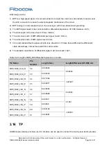
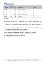
power, interrupt, reset pins. The pin definition of the module is shown in the follow table: 

Table 3-21 TP pin definition 

Pin Name 

Pin Number 

I/O 

Description 

Note 

TP_INT 

30 

DI 

LCD TP interrupt signal 

TP_RST 

31 

DO 

LCD TP reset signal 

VDD1V85 

111 

PO 

LCD TP IO voltage output 

VDD2V8 

228 

PO 

LCD TP VDD voltage output 

TP_I2C_SCL 

47 

DO 

LCD TP I2C clock 

TP_I2C_SDA 

48 

I/O 

LCD TP I2C data 

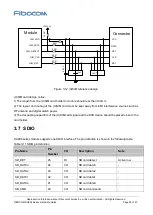
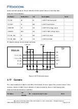
TP reference design circuit is shown as follows: 

TS_I2C_SCL

TS_I2C_SDA

TP_RST

  TP_INT

SCL

SDA

VDD1V85

RESET

INT

VDD

NC

10

K

NC

VDD2V8

100nF

2.2uF

TP

Module


Figure 3-16 TP reference design 

3.17    Camera 

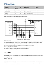
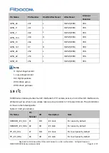
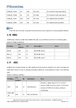
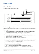
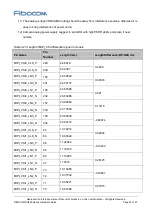
The camera interface is based on the MIPI_CSI standard and can support three (4-lane+2-lane+1-lane) 

cameras, maximum 13MP. The pin definition of camera interface is shown in the following table: 

Table 3-22 Camera interface pin definition 

Pin Name


Pin 

Number


I/O


4-Lane+2-Lane+1-Lane


Note 

Summary of Contents for SU806 Series

Page 1: ...FIBOCOM SU806 Series Hardware Guide Version V2 0 0 Date 2021 02 01...

Page 2: ...AM 4G frequency Android 10 applicable to China 2 SU806 CN 01 8GB e MMC 8Gb LPDDR3 SDRAM 4G frequency diversity removal Android 9 applicable to China 3 SU806 CN 11 16GB e MMC 16Gb LPDDR3 SDRAM 4G frequ...

Page 3: ...vidual is prohibited to excerpt copy any part of or the entire document or transmit the document in any form Notice The document is subject to update from time to time owing to the product version upg...

Page 4: ...ghts Reserved FIBOCOM SU806 Series Hardware Guide Page 4 of 91 Change History Version Author Reviewer Approver Update Date Description V2 0 0 Mo Xiaoke He Sihai Tu Min Li Xiyi Chen Guojiang 2021 02 01...

Page 5: ...on 12 2 3 Functional Block Diagram 14 2 4 Pin Definition 16 2 4 1 Pin Assignment 16 2 4 2 Pin Descriptions 17 3 Application Interface 27 3 1 Power Supply 27 3 1 1 Power Input 27 3 1 2 VRTC 28 3 1 3 Po...

Page 6: ...arpiece Circuit Design 55 3 19 4 Headset Circuit Design 56 3 19 5 Speaker Circuit Design 56 3 20 Force Download Interface 57 4 Antenna Interface 58 4 1 MAIN DRX Antenna 58 4 1 1 Operating Band 58 4 1...

Page 7: ...70 8 2 Absolute Maximum Ratings 70 8 3 Power Consumption 70 8 4 RF Transmit Power 77 8 5 RF Receiver Sensitivity 79 8 6 Electrostatic Protection 82 9 Structural Specification 83 9 1 Product Appearance...

Page 8: ...Radio transmission and reception TDD 3GPP TS 36 521 1 V10 6 0 User Equipment UE conformance specification Radio transmission and reception Part 1 Conformance testing 3GPP TS 21 111 V10 0 0 USIM and I...

Page 9: ...n be determined by turning the equipment off and on the user is encouraged to try to correct the interference by one or more of the following measures Reorient or relocate the receiving antenna Increa...

Page 10: ...cated or operating in conjunction with any other antenna or transmitter The module is limited to OEM installation ONLY The OEM integrator is responsible for ensuring that the end user has no manual in...

Page 11: ...I USB UART SPI I2C It is the optimal solution for the core system of wireless smart products Its corresponding network modes and frequency bands are as follows Table 2 1 Bands supported of SU806 CN Mo...

Page 12: ...3 8V Application processor Quad core ARM CortexTM A53 MP processor up to 1 4GHz Memory 8GB e MMC 8Gb LPDDR3 16GB e MMC 16Gb LPDDR3 Power class Class 4 33dBm 2dB for GSM850 EGSM900 Class 1 30dBm 2dB fo...

Page 13: ...and MT SMS cell broadcast SMS storage stored in the module by default LCD interface One 4 lane MIPI_DSI interface Support maximum HD 60fps 1440x720 Camera interface Two 4 lane MIPI_CSI interface can s...

Page 14: ...face One universal 12bits ADC RTC Support Antenna interface MAIN antenna DRX antenna GNSS antenna WIFI BT antenna Physical characteristics Dimension 40 5mm 40 5mm 2 8mm Encapsulation 146 LCC pin 116 L...

Page 15: ...IM card interface MIPI DSI interface MIPI CSI Interface Analog audio interface Baseband PMU TXM Duplex SAW Transceiver LCM UART TP ADC RESET PWRKEY 26M XO VBAT SAW PA ANT_MAIN ANT_DIV ANT_GNSS Tx PRx...

Page 16: ...authorization All Rights Reserved FIBOCOM SU806 Series Hardware Guide Page 16 of 91 2 4 Pin Definition 2 4 1 Pin Assignment Figure 2 2 Pin assignment top view Note NC represent No Connect the pin of...

Page 17: ...og Output OD Open Drain Pin descriptions of SU806 series module are presented in the following table Table 2 5 Pin description Pin Name Pin Number I O Functional Description Note Power supply VBAT 1 2...

Page 18: ...120 122 130 132 135 140 143 144 147 148 149 150 160 178 180 182 184 186 188 189 192 193 198 200 201 208 209 211 218 221 235 245 246 250 251 262 Ground Battery supply interface CHARGE_SEL 127 DI Charge...

Page 19: ...2 hot plug detection Disabled by default cannot used as general GPIO UIM1_DATA 25 I O U SIM card 1 data UIM1_CLK 24 DO U SIM card 1 clock UIM1_RST 23 DO U SIM card 1 reset UIM1_DET 22 DI U SIM card 1...

Page 20: ...ont depth camera by default CAM_I2C_SDA1 240 I O I2C data For front depth camera by default USB interface USB_VBUS 141 142 PI USB 5V input USB_DP 14 AI AO USB HS data USB_DM 13 AI AO USB HS data USB_I...

Page 21: ...lay serial interface lane MIPI_DSI0_ LN0_P 55 AO MIPI_DSI0_ LN1_N 56 AO MIPI_DSI0_ LN1_P 57 AO MIPI_DSI0_LN2_N 58 AO MIPI_DSI0_LN2_P 59 AO MIPI_DSI0_LN3_N 60 AO MIPI_DSI0_LN3_P 61 AO LCD_RST 49 DO LCD...

Page 22: ...power down MIPI_CSI1_CLK_N 63 AI MIPI front camera serial interface clock MIPI_CSI1_CLK_P 64 AI MIPI_CSI1_LN0_N 65 AI MIPI front camera serial interface lane MIPI_CSI1_LN0_P 66 AI MIPI_CSI1_LN1_N 67...

Page 23: ...one PA ground sensing HPH_R 136 AO Headphone PA right channel output HPH_DET 139 AI Headset detection MIC2_P 6 AI Headset MIC difference input MIC1_M 5 AI MIC1 difference input MIC1_P 4 AI MIC1 differ...

Page 24: ...e enable The module does not support charging and DC DC circuit can be added if charging function is required ADC4_BAT_ID 260 AI BAT_ID detection NFC_CLK 256 DO NFC clock Reserved NFC_DWL_REQ 257 DI N...

Page 25: ...UT WPU GPIO_140 124 I O INPUT WPU GPIO_88 153 I O INPUT WPU GPIO_30 159 I O INPUT WPD GPIO_29 183 I O INPUT WPD GPIO_27 187 I O INPUT WPD GPIO_85 202 I O OUTPUT GPIO_154 203 I O INPUT WPD GPIO_155 205...

Page 26: ...I O Functional Description Note NC NC 154 191 197 199 204 222 to 224 247 to 249 255 Keep floating Note H High voltage tolerant L Low voltage tolerant Hiz High impedance WPU Weak pull up WPD Weak pull...

Page 27: ...The VBAT voltage drop is shown as the following figure Burst Transmit Burst Transmit VBAT 3 5V 3 0V Drop 500mV Figure 3 1 VBAT voltage drop 3 1 1 Power Input External power source supplies the module...

Page 28: ...ion it is required to adopt low ESR capacitor LDO or DCDC power requires not less than 440uF capacitor Battery power can be properly reduced to 100 220uF capacitor 1uF 100nF Filter capacitor Filter cl...

Page 29: ...design 3 1 3 Power Output The SU806 series module provides multiple power outputs for peripheral circuits It is recommended to connect 33pF and 10pF capacitors in parallel with every power to avoid h...

Page 30: ...nd sleep wake up Its pin definition is shown as follow table Table 3 5 Power on off signal Pin Name Pin Number I O Description Note KEY_PWR_ON 114 DI Active low module power on off restart sleep wake...

Page 31: ...Powers Figure 3 6 Power on timing 3 2 1 2 Power off Normal power off when module in operating mode pull down KEY_PWR_ON pin 0 6s 6s user interface will display selection box select power off or restar...

Page 32: ...ON pin 7s 10s module will be forced reset The reset timing is shown as follows 7s t 10s KEY_PWR_N DCDCGEN1V85 VBAT 7s Figure 3 7 Force reset timing Two key KEY_PWR_ON KEY_RESIN_N reset when module in...

Page 33: ...6 USB2 0 pin definition Pin Name Pin Number I O Description Note USB_VBUS 141 142 PI USB VBUS 5V input USB_DP 14 AI AO USB HS data USB_DM 13 AI AO USB HS data USB_ID 16 DI USB OTG detection The refer...

Page 34: ...mission rate is 480Mbps Please pay attention to the following requirements in PCB layout USB_DP and USB_DM signal cables are required to be parallel and equal in length differential cable length contr...

Page 35: ...DO UART0 data transmission UART0_RX 35 DI UART0 data reception UART0_CTS 36 DI UART0 clear to send UART0_RTS 37 DO UART0 request to send UART1_TX 94 DO UART1 data transmission Debug_UART serial port...

Page 36: ...Figure 3 10 Level shift reference design The other level translator circuit is shown as Figure 3 11 The rest input and output circuit design of dotted line please refer to solid line part but pay att...

Page 37: ...rt hot plug default off Table 3 10 U SIM pin definition Pin Name Pin Number I O Description Note UIM1_DATA 25 I O U SIM 1 data signal UIM1_CLK 24 DO U SIM 1 clock signal UIM1_RST 23 DO U SIM 1 reset s...

Page 38: ...layout and routing of the U SIM card must be kept away from EMI interference sources such as RF antenna and digital switch power 3 The decoupling capacitors of the U SIM card signal and the ESD devic...

Page 39: ...22R 22R 22R 22R 22R DETECTIVE NC NC NC NC NC VDD1V85 4 7uF 100nF NC VDDSDCORE Connector 22R VDD 100K 100MHz_120R Figure 3 13 SDIO reference design SDIO design notice 1 VDDSDCORE is the SD card periphe...

Page 40: ...IO_131 101 L INPUT WPD YES GPIO_130 102 L INPUT WPD YES GPIO_133 103 L INPUT WPD YES GPIO_132 104 L INPUT WPD YES GPIO_121 105 L OUTPUT YES GPIO_138 106 H INPUT WPU YES GPIO_91 108 L INPUT WPD YES GPI...

Page 41: ...NPUT WPD YES Note H High voltage tolerant L Low voltage tolerant Hiz High impedance WPU Weak pull up WPD Weak pull down 3 9 I2 C SU806 series module provides four I2C interfaces for TP camera sensor e...

Page 42: ...es three RGB LED inputs its pin definition is shown in the following table Table 3 14 RGB pin definition Pin Name Pin Number I O Description Note LED_B 194 AI RGB LED input 2 LED_G 195 AI RGB LED inpu...

Page 43: ...Reserved VBAT_SNS 133 AI Battery voltage sense VBAT_THERM 134 AI Battery thermal detect input NTC resistor is 47K SENSE_N 258 AI Battery fuel gauge negative input Reserved SENSE_P 259 AI Battery fuel...

Page 44: ...PO Vibration motor driver output Can be configured as LDO mode and connect with Vibration motor 3 15 LCM The video output of SU806 series module can support single screen display Its screen interface...

Page 45: ...DO LCD reset PWM 29 DO LCD backlight PWM LCD_TE 50 DI LCD tearing effect Keep floating if unused GPIO_25 190 DO LCD backlight enable The reference design of LCD interface circuit is shown as follows...

Page 46: ...mm 6 The inter lane match of MIPI signal must 2mm 7 It is recommended that the space of intra lane should be 1 5 times trace width and the differential cable should keep 3 times trace width from other...

Page 47: ...ltage output VDD2V8 228 PO LCD TP VDD voltage output TP_I2C_SCL 47 DO LCD TP I2C clock TP_I2C_SDA 48 I O LCD TP I2C data TP reference design circuit is shown as follows TS_I2C_SCL TS_I2C_SDA TP_RST TP...

Page 48: ...camera serial interface lane 0 MIPI_CSI0_LN1_P 156 AI MIPI rear camera serial interface lane 1 MIPI_CSI0_LN1_N 232 AI MIPI rear camera serial interface lane 1 MIPI_CSI0_LN2_P 157 AI MIPI rear camera s...

Page 49: ...clock SCAM_RST 81 DO Front camera reset SCAM_PWDN 82 DO Front camera power down MIPI_CSI1_LN3_N 70 AI MIPI depth camera serial interface clock MIPI_CSI1_LN3_P 71 AI MIPI depth camera serial interface...

Page 50: ...ST SCL SDA DAT2_N DAT0_P DAT0_N VDD1V85 NC NC VDDCAMA AVDD AFVDD DVDD VCCCAMMOT VDDCAMCORE DOVDD VDD1V8 1uF 10uF 1uF EMI EMI EMI EMI EMI 100nF 100nF 10uF Figure 3 17 Rear camera reference design 3 17...

Page 51: ...de inductor in series near the LCD connector to reduce the electromagnetic interference of the circuit 2 MIPI routing is recommended to be in the inner layer with three dimensional grounding 3 The MIP...

Page 52: ...ength Difference DP DM mm MIPI_CSI0_CLK_P 229 24 6976 0 2409 MIPI_CSI0_CLK_N 230 24 4567 MIPI_CSI0_LN0_P 155 24 59549 0 09393 MIPI_CSI0_LN0_N 231 24 50157 MIPI_CSI0_LN1_P 156 24 65386 0 021 MIPI_CSI0_...

Page 53: ...d proximity sensor interrupt MAG_RST 109 DO Magnetic sensor reset ACCL_INT 110 DI Accelerometer sensor interrupt 3 19 Audio 3 19 1 Audio Interface Pin Definition SU806 series module supports analog au...

Page 54: ...er externally it is recommended to connect 8 speakers Note that the route width must meet the power rating requirements If an external audio amplifier is required please use the output of headphone as...

Page 55: ...hts Reserved FIBOCOM SU806 Series Hardware Guide Page 55 of 91 3 19 2 Microphone Circuit Design Module MIC_M MIC_P 33pF 33pF 100pF Figure 3 20 Microphone reference design 3 19 3 Earpiece Circuit Desig...

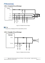
Page 56: ...rdware Guide Page 56 of 91 3 19 4 Headset Circuit Design HPH_R 0R 33pF HPH_L HPH_GND HPH_DET MIC2_P 1K Module 33pF 33pF Figure 3 22 Headset reference design Note Please choose bidirectional TVS for he...

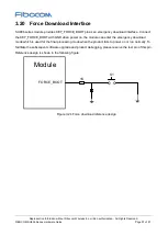
Page 57: ...download interface Connect the KEY_FORCE_BOOT with GND when power on the module can enter the emergency download mode which is used for the final processing mode when the product fails to power on or...

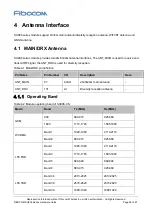
Page 58: ...signal the ANT_DRX is used for diversity reception Table 4 1 Main DRX pin definition Pin Name Pin Number I O Description Note ANT_MAIN 87 AI AO 2G 3G 4G main antenna ANT_DRX 131 AI Diversity reception...

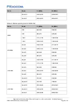
Page 59: ...z Rx MHz GSM 850 824 849 869 894 900 880 915 925 960 1800 1710 1785 1805 1880 1900 1850 1910 1930 1990 WCDMA Band 1 1920 1980 2110 2170 Band 2 1850 1910 1930 1990 Band 5 824 849 869 894 Band 8 880 915...

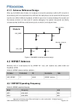
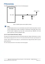
Page 60: ...e antenna connector or feed point for antenna debugging Two parallel components are directly connected across the RF trace and should not pull out a branch as the figure shows Module ANT_MAIN ANT_DRX...

Page 61: ...GNSS supports GPS BeiDou Table 4 6 GNSS antenna interface definition Pin Name Pin Number I O Description Note ANT_GNSS 121 AI GNSS antenna 4 3 1 Operating Frequency Table 4 7 GNSS operating frequency...

Page 62: ...ity of resist ESD For better ability of resist ESD please choose TVS that junction capacitance less than 0 5pF recommended type ESD9D5U with 0 5pF junction capacitance and 5 0V embedded voltage 4 3 2...

Page 63: ...four antenna interfaces main diversity WIFI BT and GNSS The antenna requirements are as follows Table 4 8 Antenna requirements SU806 Series Module Antenna Requirement Standard Antenna Requirement GSM...

Page 64: ...SU806 Series Hardware Guide Page 64 of 91 SU806 Series Module Antenna Requirement Standard Antenna Requirement GNSS Frequency range 1559MHz 1607MHz Polarization type right circular or linear polariza...

Page 65: ...material the trace width W the ground clearance S and the height of the reference ground plane H The control of the characteristic impedance of the PCB usually in two ways microstrip trace and coplana...

Page 66: ...l cable at 50 impedance The GND pin adjacent to the RF pin should not have thermal welding plate and should be in full contact with the ground The distance between the RF pin and the RF connector shou...

Page 67: ...upport Wake on WLAN WoWLAN Support ad hoc mode Support WAPI Support AP mode Support Wi Fi Direct Support MCS 0 7 for HT20 6 2 WIFI Performance Test condition 3 8V power supply environment temperature...

Page 68: ...bandwidth is 2MHz and can accommodate 40 channels Its main features are as follows BT 4 2 BR EDR BLE Support for ANT protocol Support for BT WLAN coexistence operation including optional concurrent r...

Page 69: ...oning systems The module is embedded with LNA which can effectively improve the sensitivity of GNSS 7 2 Performance Test condition 3 8V power supply environment temperature 25 C Table 7 1 GNSS positio...

Page 70: ...atings The functionality of SU806 series module is subject to the absolute maximum minimum values listed in the following table Do not exceed these parameters or the part may be damaged permanently Op...

Page 71: ...g Cycle 256 TBD Radio Off AT CFUN 4 Flight Mode TBD IGSM RMS GSM voice RMS Current EGSM900 PCL 5 TBD mA EGSM900 PCL 19 TBD DCS1800 PCL 0 TBD DCS1800 PCL 15 TBD IGSM MAX GSM voice Peak current EGSM900...

Page 72: ...er 10MHz 1RB TBD Band40 max power 10MHz 1RB TBD Band41 max power 10MHz 1RB TBD Table 8 4 SU806 CN 01 SU806 CN 11 power consumption Parameter Description Condition Typical Result Unit Ioff Static leaka...

Page 73: ...L 4DL 161 DCS1800 Gamma 5 4UL 1DL 468 IWCDMA RMS WCDMA RMS Current Band1 max power 589 mA Band8 max power 598 ILTE RMS FDD data RMS Current Band1 max power 10MHz 1RB 595 mA Band3 max power 10MHz 1RB 6...

Page 74: ...MS Current EGSM900 PCL 5 256 mA EGSM900 PCL 19 90 DCS1800 PCL 0 196 DCS1800 PCL 15 89 IGSM MAX GSM voice Peak current EGSM900 PCL 5 2100 mA DCS1800 PCL 0 1300 IGPRS RMS GPRS data RMS Current EGSM900 G...

Page 75: ...r 10MHz 1RB 322 Band40 max power 10MHz 1RB 342 Band41 max power 10MHz 1RB 354 Table 8 6 Power consumption of SU806 EAU 00 Parameter Description Condition Typical Result Unit Ioff Static leakage curren...

Page 76: ...mA EGSM900 PCL 5 TBD DCS1800 PCL 0 TBD PCS1900 PCL 0 TBD IGPRS RMS GPRS data RMS current GSM850 Gamma 3 1UL 4DL TBD mA GSM850 Gamma 3 4UL 1DL TBD EGSM900 Gamma 3 1UL 4DL TBD EGSM900 Gamma 3 4UL 1DL T...

Page 77: ...D mA Band3 max power 10MHz 1RB TBD Band5 max power 10MHz 1RB TBD Band7 max power 10MHz 1RB TBD Band8 max power 10MHz 1RB TBD Band20 max power 10MHz 1RB TBD Band28 max power 10MHz 1RB TBD TDD data RMS...

Page 78: ...3 49 LTE FDD Band 1 23 0 2 39 Band 3 23 0 2 39 Band 5 23 0 2 39 Band 8 23 0 2 39 LTE TDD Band 34 23 0 2 39 Band 38 23 0 2 39 Band 39 23 0 2 39 Band 40 23 0 2 39 Band 41 23 0 2 39 Table 8 8 RF Transmit...

Page 79: ...2 39 8 5 RF Receiver Sensitivity The sensitivity of each frequency band of the SU806 series module is shown in the following table Test condition 3 8V power supply environment temperature 25 C The te...

Page 80: ...ensitivity of SU806 CN 01 SU806 CN 11 Mode Band Primary Diversity PRX Div 3GPP Requirement Unit GSM 900 109 102 dBm 1800 108 8 102 dBm WCDMA Band 1 110 106 7 dBm Band 8 110 5 103 7 dBm LTE FDD Band 1...

Page 81: ...4 99 2 102 1 93 3 dBm LTE TDD Band 34 97 2 97 3 100 4 96 3 dBm Band 38 96 5 96 8 99 6 96 3 dBm Band 39 97 97 5 100 5 96 3 dBm Band 40 96 3 97 100 96 3 dBm Band 41 95 8 96 5 99 2 94 3 dBm Table 8 12 R...

Page 82: ...between micro electronics etc discharging to the module through various channels that may cause damage so ESD protection should be taken seriously attention In the process of R D production assembly...

Page 83: ...are Guide Page 83 of 91 9 Structural Specification 9 1 Product Appearance SU806 series module product appearance is shown in the following figure Figure 9 1 Module product appearance 9 2 Structural Di...

Page 84: ...Wireless Inc written authorization All Rights Reserved FIBOCOM SU806 Series Hardware Guide Page 84 of 91 9 3 PCB Soldering Pad and Stencil Design PCB soldering pad and stencil design please refer to...

Page 85: ...IBOCOM SU806 Series Hardware Guide Page 85 of 91 10 Production and Storage 10 1 SMT SMT production process parameters and related requirements please refer to FIBOCOM Sx806 Series SMT Design Guide 10...

Page 86: ...continuous Reception EGSM Extended GSM900 Band FDD Frequency Division Duplexing GMSK Gaussian Minimum Shift Keying GSM Global System for Mobile Communications HSDPA High Speed Down Link Packet Access...

Page 87: ...RHCP Right Hand Circularly PolarizedRMS RMS Root Mean Square RTC Real Time Clock Rx Receive SMS Short Message Service TDMA Time Division Multiple Access TE Terminal Equipment TX Transmitting Direction...

Page 88: ...Value VILmax Maximum Input Low Level Voltage Value VILmin Minimum Input Low Level Voltage Value VImax Absolute Maximum Input Voltage Value VImin Absolute Minimum Input Voltage Value VOHmax Maximum Out...

Page 89: ...Page 89 of 91 Appendix B GPRS Encoding Scheme Table B 0 1 GPRS encoding scheme Encoding method CS 1 CS 2 CS 3 CS 4 Rate 1 2 2 3 3 4 1 USF 3 3 3 3 Pre coded USF 3 6 6 12 Radio Block excl USF and BCS 1...

Page 90: ...rate of uplink and downlink The expression is 3 1 or 2 2 the first number represents the number of downlink timeslots and the second number represents the number of uplink timeslots Active timeslot r...

Page 91: ...GMSK 9 05kbps 18 1kbps 36 2kbps CS 2 GMSK 13 4kbps 26 8kbps 53 6kbps CS 3 GMSK 15 6kbps 31 2kbps 62 4kbps CS 4 GMSK 21 4kbps 42 8kbps 85 6kbps MCS 1 GMSK C 8 80kbps 17 6kbps 35 2kbps MCS 2 GMSK B 11...

Reviews: