background image

L831-EA Module Hardware User Manual

Page 30 of 43

5.5.1 USIM Pins

Pin#

Name

Type

Description

36

UIM_PWR

O

USIM power supply signal

30

UIM_RESET

O

USIM Reset signal

32

UIM_CLK

O

USIM clock signal

34

UIM_DATA

I/O

USIM data signal

66

SIM_DETECT

I

The detection signal for SIM insetting

The default is 390K ohm resistance pulled up and

input.

High level: SIM is present.

Low level: SIM is absent

5.5.2 Description of USIM

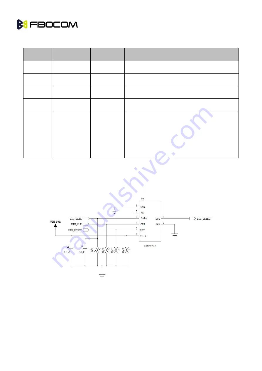
5.5.2.1 “Normally Closed

SIM Circuit Design

Referenced Circuit Design:

Figure5- 7 Reference Design of “Normally Closed” SIM Card Interface

Normally closed SIM Connector:

1

Pull out SIM card, pin 7 and pin 8 short-circuit .

2

Insert SIM card, pin 7 and pin 8 disconnect.

Summary of Contents for L-831-EA

Page 1: ...ng L831 EA Module Hardware User Manual Version V1 0 1 Date 2015 02 12...

Page 2: ...n to other parties is prohibited without the written consent of Fibocom Copyright Copy Reproduce Distribute and or Edit of this document or part of it as well as utilization of its contents and commun...

Page 3: ...r television reception which can be determined by turning the equipment off and on the user is encouraged to try to correct the interference by one or more of the following measures Reorient or reloca...

Page 4: ...ronment can be satisfied The end user has to also be informed that any changes or modifications not expressly approved by the manufacturer could void the user s authority to operate this equipment If...

Page 5: ...L831 EA Module Hardware User Manual Page 5 of 43 Revision History Version Date Remarks V1 0 0 2014 12 30 Initial version V1 0 1 2015 02 12 Update the consumption and the power on off timing...

Page 6: ...al Page 6 of 43 Applicability Table No Type Note 1 L831 EA The difference of L831 EA wireless module as listed below Model Type LTE FDD WCDMA GSM GPRS EDGE L831 EA Band 1 2 3 4 5 7 8 13 17 18 19 20 Ba...

Page 7: ...4 1 Pins Definition 19 4 1 1 Pins Number 19 4 1 2 Pins Description 20 5 Hardware Interface 24 5 1 Power Interface 24 5 1 1 Power Supply 24 5 1 2 VSD2_1V8 24 5 2 Power on off and Reset Signal 25 5 2 1...

Page 8: ...34 5 8 W_DISABLE Interface 34 5 8 1 Description of WWAN_DISABLE Interface 34 5 8 2 Description of GPS_DISABLE Interface 35 5 9 TX_BLANKING Interface 35 5 10 The WAKEUP_HOST Interface 35 5 11 BODY_SAR...

Page 9: ...L831 EA Module Hardware User Manual Page 9 of 43 7 2 2 Impedance Design 42 7 3 Antenna Design 42 7 3 1 Antenna Design Requirements 42...

Page 10: ...ort on mobile radio interface 3GPP TS 27 010 v6 0 0 Terminal Equipment to User Equipment TE UE multiplexer protocol 3GPP TS 27 060 v6 0 0 Packet domain Mobile Station MS supporting Packet Switched ser...

Page 11: ...9 5 0 Base Station BS and repeater ElectroMagnetic Compatibility EMC 3GPP TS 36 124 V9 2 0 ElectroMagnetic Compatibility EMC requirements for mobile terminals and ancillary equipment 3GPP TS 36 133 V9...

Page 12: ...20 WCDMA HSPA Band 1 2 4 5 8 GSM GPRS EDGE 850 900 1800 1900MHz Data LTE FDD Category 4 150Mbps DL 50Mbps UL UMTS HSDPA HSUPA 3GPP Rel 8 DC HSDPA 42Mbps Cat24 42Mbps Cat20 HSUPA 11 5Mbps Cat7 GSM 3GP...

Page 13: ...otocol stack EDGE Multi slot class 33 5 Down 4 Up 6 Total Coding Scheme MCS1 9 GPRS Multi slot class 33 5 Down 4 Up 6 Total Coding Scheme MCS1 4 CSD UMTS 14 4kbps GSM 9 6kbps USSD Support SMS MO MT Te...

Page 14: ...2 The minimum distance between the user and or any bystander and the radiating structure of the transmitter is 20cm 3 Assessment of compliance of the product with the requirements relating to the Radi...

Page 15: ...L831 EA Module Hardware User Manual Page 15 of 43 2 3 Appearance The following pictures show the L831 EA wireless module Top view Figure 2 1 Top View Bottom view Figure 2 2 Bottom View...

Page 16: ...L831 EA Module Hardware User Manual Page 16 of 43 3 Mechanical 3 1 Dimension Figure3 1Dimension Diagram...

Page 17: ...the size of the module please refer to the section3 1 As shown in Figure 4 2 L831 EA module uses the 75 pin fingers interface 67pin is the signal interface and Pin8 is notch About the naming rules of...

Page 18: ...of 43 3 3 M 2 Connector Recommend to use the M 2 connector from LOTES the type is APCI0026 P001A the package of connector design please refer to the relevant specifications As shown in Figure 3 2 Figu...

Page 19: ...51 50 NC NC 49 48 TX_BLANKING NC 47 46 SYSCLK GND 45 44 GNSS_IRQ NC 43 42 GNSS_SDA NC 41 40 GNSS_SCL GND 39 38 NC SSIC TXP USB3 0 TX NC 37 36 UIM_PWR SSIC TXN USB3 0 TX NC 35 34 UIM_DATA GND 33 32 UIM...

Page 20: ...3 3V PI The main power input the voltage range is 3 135V 4 4V 5 GND GND 6 FUL_CARD_POWER_OFF I PU PU Off control signal the internal 200K ohm will be pulled down CMOS 1 8V 7 USB D I O USB 2 0 signal...

Page 21: ...nel clock signal CMOS 1 8V 29 SSIC RXN USB3 0 RX NC NC 30 UIM_RESET O PP PP Reset signal of USIM card 31 SSIC RXP USB3 0 RX NC I O NC 32 UIM_CLK O PP PP Clock signal of USIM card 33 GND GND 34 UIM_DAT...

Page 22: ...GND GND 52 NC NC 53 NC NC 54 NC NC 55 NC NC 56 NC NC 57 GND GND 58 NC NC 59 ANTCTL0 O Tunable antenna control signal GPO CMOS 1 8V not support yet 60 NC NC 61 ANTCTL1 O L L Tunable antenna control sig...

Page 23: ...power input the voltage range is 3 135V 4 4V 71 GND GND 72 3 3V PI The main power input the voltage range is 3 135V 4 4V 73 GND GND 74 3 3V PI The main power input the voltage range is 3 135V 4 4V 75...

Page 24: ...mmended capacitor Application Description 330uF Supply capacitor Reduce power wave in call The value of capacitor is bigger better 1uF 100nF Digital signal noise Filtering interference from clock and...

Page 25: ...1 Power on off Signal 5 2 1 1 Power on Clients can pull up the FUL_CARD_POWER_OFF signal while the module is power on then the module will turn on The Pulse Timing requirements as listed below Parame...

Page 26: ...While pulling down the FUL_CARD_POWER_OFF signals or floating the modules PMU Power Management Unit will be reset then the module will get into off modes from working modes Note the RESET_N signal mus...

Page 27: ...PMU cannot power cut while the clients execute the RESET function Note Reset signal is sensitive signal line while PCB layout please keep it away from RF interference add the surrounding processing a...

Page 28: ...index 5 4 USB Interface 5 4 1 Definition of USB Interface Pin No Pin Name I O Description 7 USB_DP I O USB signal 8 USB_DM I O USB signal L831 EA wireless module supports USB 2 0 It should be install...

Page 29: ...he VBUS pin of Host end can float USB_D and USB_D is high speed differential signal line the highest transmit speed is up to480Mbps Not the following requirements while PCB Layout USB_DP and USB_D sig...

Page 30: ...TECT I The detection signal for SIM insetting The default is 390K ohm resistance pulled up and input High level SIM is present Low level SIM is absent 5 5 2 Description of USIM 5 5 2 1 Normally Closed...

Page 31: ...ignal need add ESD protection just like TVS pipe ESD components should be closed to SIM card pin SIM_CD signal connection supports hot plug default high level is available switch to low level is avail...

Page 32: ...ECT signal connects Pin8 SW2 of U2 and pull down to ground through 47Kohm resistance Pin 7 SW1 shall be pulled up with4 7Kohms SW2 and SW1 is disconnected while SIM card is not inserted so SW2 is low...

Page 33: ...Hz 44 1KHz 32KHz 24KHz 22 5KHz 16KHz 12KHz 11 025KHz 8KHz 5 6 2 Description of PCM Interface L831 EA Signal Direction Audio CODEC PCM Port I2S_CLK0 PCM_CLK PCM clock signal PCM_CLK PCM clock signal I2...

Page 34: ...S_IRQ signal as listed below No GNSS_IRQ Function 1 High Floating Support Win8 system the module s USB ports shall set as MBIM modes 2 Low Support Android system the module s USB ports shall set as 3A...

Page 35: ...ut low level by default the TX_BLANKING output the pulse signal that synchronized with GSM burst timing while the module works in GSM band Cause GSM transmitting may interfere the receiving of GPS sig...

Page 36: ...interface default configuration is I2C master The I2C can used for driving external 12C slave device such as Audio codes and so on Pin Name I O Description 42 GNSS_SDA I O I2C control signal input out...

Page 37: ...and Main Host Interface Port Configuration GND GND GND GND SSD SATA N A GND GND N C GND WWAN PCIe N A GND GND GND N C WWAN USB3 0 0 5 15 RF Interface 5 15 1Description of RF Connector L831 EA module...

Page 38: ...l Page 38 of 43 Figure 5 10 Structure diagram of RF connecting seat Figure 5 11 0 81mm coaxial line Figure 5 12 RF connector insert into RF connecting seat 5 15 3Main Performance of RF Connector Rated...

Page 39: ...e Hardware User Manual Page 39 of 43 Frequency range DC to 6GHz Temperature range Characteristic impedance 50 40 C to 85 C 5 16 Other Interfaces The following interfaces are not supported now GPIO and...

Page 40: ...e electrical features range of L831 EA module Parameter Minimum Value Maximum Value Unit Power supply 0 4 4 V Digital Signal 0 1 9 V 6 2 Environmental This table shows the environmental features of L8...

Page 41: ...D WCDMA GSM 880 915 925 960 Band 13 US 700MHz blocks C LTE FDD 777 787 746 756 Band 17 US 700MHz blocks B C LTE FDD 704 716 734 746 Band 18 Japan 850MHz LTE FDD 815 830 860 875 Band 19 Japan Extend 85...

Page 42: ...y antenna is different from main antenna 4 Radiation Pattern Radiation pattern is the antenna s electromagnetic field strength in all directions of far field Half wave dipole antenna is the most suita...

Page 43: ...P Total Radiated Power GSM850 900 28dBm GSM DCS1800 PCS1900 25dBm WCDMA Band 1 2 4 5 8 19dBm LTE FDD Band 1 2 3 5 7 8 13 17 18 19 20 19dBm TIS Total Isotropic Sensitivity GSM850 GSM 900 DCS1800 PCS190...

Reviews: