H350 LGA Serials Module Hardware User Manual Page 10 of 37
3
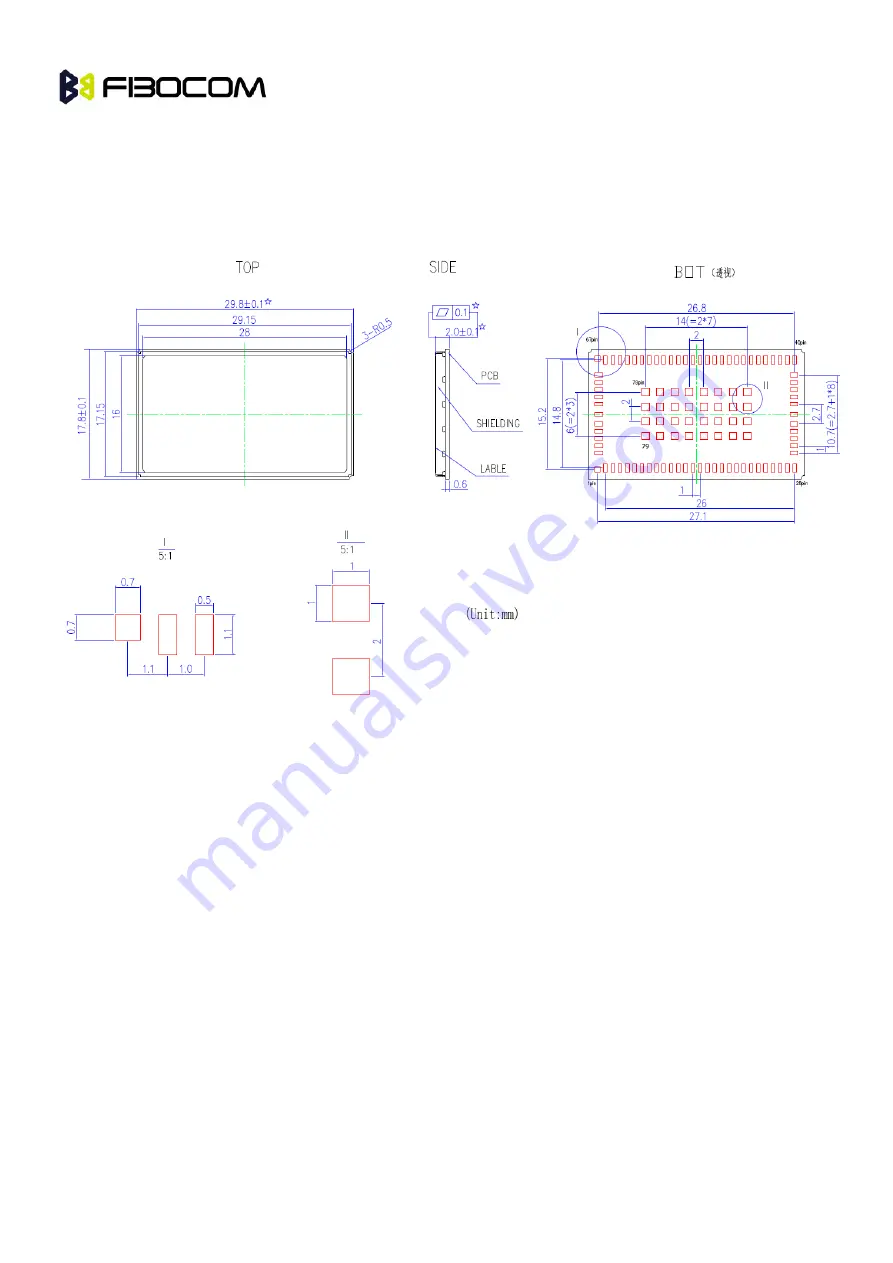
Mechanical
3.1
Dimensions
Figure 3-1 Mechanical Specifications
Page 1: ...H350 LGA Serials Module Hardware User Manual Version V1 0 1 Date 2013 10 23 ...
Page 2: ...opy Reproduce Distribute and or Edit of this document or part of it as well as utilization of its contents and communication thereof to others without express authorization are prohibited Offenders will be held liable for payment of damages All rights created by patent grant or registration of a utility model or design patent are reserved Copyright 2013 Fibocom Wireless Inc All rights reserved Tra...
Page 3: ...ge 3 of 37 Applicability Table No Type Note 1 H350 A50 00 2 H350 A30 00 Here are the module comparisons Model No GSM GPRS EDGE Band MHz WCDMA Band MHz HSDPA Mbps HSUPA Mbps H350 A30 00 900 1800 900 2100 7 2 5 76 H350 A50 00 900 1800 900 2100 21 5 76 ...
Page 4: ... 12 4 1 Block Diagram 12 4 2 Pin Definition 13 4 2 1 Pin Map 13 4 2 2 Pin Description 14 5 Hardware Interface 19 5 1 Power Interface 19 5 1 1 VBAT 19 5 1 2 Power Consumption 19 5 1 3 VIO 21 5 1 4 VRTC 21 5 2 ON OFF and Reset 22 5 2 1 Pin Definition 22 5 2 2 Power ON Signal 22 5 2 3 Power off Signal 23 5 2 4 Reset Signal 24 5 3 Indicator Signal 25 5 3 1 Pin Description 25 5 3 2 Indicator Descriptio...
Page 5: ...3 USIM Design Notice 30 5 6 4 USIM Hot Plug 31 5 7 Digital Audio 31 5 7 1 I2S 32 5 7 2 I2C 32 5 7 3 PCM Mode Interface 32 5 8 ADC Interface 33 5 9 Others 33 6 Electrical and Environmental Features 34 6 1 Electrical Features 34 6 2 Environmental Features 34 7 RF Interface 35 7 1 Operation Frequency Band 35 7 1 1 Main Antenna 35 7 2 RF PCB Design 35 7 2 1 Layout Guideline 35 7 2 2 Impedance 35 7 3 A...
Page 6: ... Equipment TE UE multiplexer protocol 3GPP TS 27 060 v6 0 0 Packet domain Mobile Station MS supporting Packet Switched services 3GPP TS 25 304 v6 10 0 User Equipment UE procedures in idle mode and procedures for cell reselection in connected mode 3GPP TS 25 308 v6 4 0 High Speed Downlink Packet Access HSDPA Overall description Stage 2 3GPP TS 25 309 v6 6 0 FDD enhanced uplink Overall description S...
Page 7: ...ps Cat 8 GSM 3GPP release 7 EDGE E GPRS multi slot class 33 296kbps DL 236 8kbps UL GPRS multi slot class 33 67kbps DL 53 6kbps UL Physical Dimension 29 8mm x 17 8mm x 2 00mm Interface LGA Weight 2 5 grams Environment Operating Temperature 30 85 Storage Temperature 40 85 Performance Operating Voltage Voltage 3 3V 4 2V Normal 3 8V Operating Current Typical Value 2mA Sleep Mode 3G Idle 13mA 3G Talk ...
Page 8: ...GPIO A D RTC Data Features Protocol Stack Embedded TCP IP and UDP IP protocol stack EDGE Multi slot class 33 5 Down 4 Up 6 Total Coding Scheme MCS1 9 GPRS Multi slot class 33 5 Down 4 Up 6 Total Coding Scheme CS1 4 CSD UMTS 14 4kbps GSM 9 6kbps USSD Support SMS MO MT Text and PDU modes Cell broadcast Voice Features Digital Audio Voice coders EFR HR FR AMR Audio Control Gain Control Character Set I...
Page 9: ...al Page 9 of 37 GSM 07 07 Accessories Firmware Loader Tool over USB UART User Manual Developer Kit 2 3 Appearance The following picture shows the H350 Wireless Communication Module Top view Figure 2 1 Top View Bottom view Figure 2 2 Bottom View ...
Page 10: ...H350 LGA Serials Module Hardware User Manual Page 10 of 37 3 Mechanical 3 1 Dimensions Figure 3 1 Mechanical Specifications ...
Page 11: ...H350 LGA Serials Module Hardware User Manual Page 11 of 37 3 2 PCB Layout Design Figure 3 2 Recommended PCB Layout ...
Page 12: ...H350 LGA Serials Module Hardware User Manual Page 12 of 37 4 Hardware Overview 4 1 Block Diagram 110 pin LGA Connector Interface Figure 4 1 Block Diagram ...
Page 13: ...H350 LGA Serials Module Hardware User Manual Page 13 of 37 4 2 Pin Definition 4 2 1 Pin Map TOP View Figure 4 2 Pin Definition ...
Page 14: ...age output inside module 44 VRTC I O Backup battery power input Power ON OFF Signal 45 POWER_OFF I Power off signal 47 POWER_ON I Power on signal Reset Signal 46 RESET_ALL_N I External reset signal USIM 27 USIM_CD I USIM card insert detected Low level activated 26 USIM_VCC O USIM card supplies the power 1 8V or 3 3V 25 USIM_RST O USIM card reset 24 USIM_CLK O USIM card clock 23 USIM_DATA I O USIM ...
Page 15: ...e 32 USB_DM I O USB data line 30 USB_ID USB ID line 33 VUSB I USB Power Input 29 USB_TEST USB TEST line I2 C 20 I2C_SDA I O I2C data line 19 I2C_SCL O I2C clock line UART1 12 UART1_RI O UART1 Ring Indicator 56 UART1_DSR I UART1 DTE Ready 55 UART1_DTR O UART1 DCE Ready 57 UART1_DCD O UART1 Carrier Detect 10 UART1_CTS I UART1 Clear To Send 11 UART1_RTS O UART1 Request To Send 8 UART1_TXD O UART1 Tra...
Page 16: ...w activity USB HSIC 35 HSIC_USB_DATA HSIC USB data signal not supported 34 HSIC_USB_STRB HSIC USB pulse signal not supported Antenna 73 ANT I O antenna interface 50 ohm Impedance Others 38 CLKOUT0 O Digital audio clock output 43 SMI O Sleep Mode Indicator 54 LPG O Status Indicator 52 MIPI_HSI_RX_RDY I MIPI signal not supported 53 MIPI_HSI_TX_DATA O MIPI data not supported Not Connect 1 NC 2 NC 3 N...
Page 17: ...s Module Hardware User Manual Page 17 of 37 36 NC 37 NC 39 NC 40 NC 42 NC 58 NC GND 28 GND 60 GND 67 GND 68 GND 69 GND 70 GND 71 GND 72 GND 74 GND 75 GND 76 GND 77 GND 78 GND 79 GND 80 GND 81 GND 82 GND 83 GND 84 GND ...
Page 18: ...ardware User Manual Page 18 of 37 85 GND 86 GND 87 GND 88 GND 89 GND 90 GND 91 GND 92 GND 93 GND 94 GND 95 GND 96 GND 97 GND 98 GND 99 GND 100 GND 101 GND 102 GND 103 GND 104 GND 105 GND 106 GND 107 GND 108 GND 109 GND 110 GND ...
Page 19: ...tion Recommended capacitor Application Description 1000uF GSM Transmit current serge Minimizes power supply losses during transmit bursts Use high capacitance value as possible as you can 10nF 100nF Digital signal noise Filtering interference from clock and data sources 8 2pF 10pF 1800 1900 2100 MHz bands Filters transmission EMI 33pF 39pF 850 900 MHz bands Filters transmission EMI 5 1 2 Power Con...
Page 20: ... DCS1800 PCL 0 1012 9 5 348 7 10 141 5 15 110 3 GPRS EGSM900 PCL 5 GSM voice 1Rx slot TX slot 1 247 9 mA 4 373 7 EGSM900 PCL 10 GSM voice 1Rx slot TX slot 1 89 0 4 220 3 DCS1800 PCL 0 GSM voice 1Rx slot TX slot 1 172 4 4 259 8 DCS1800 PCL10 GSM voice 1Rx slot TX slot 1 60 3 4 101 2 EGPRS RMS EGSM900 PCL 8 GSM voice 1Rx slot TX slot 1 165 2 mA 4 493 2 EGSM900 PCL 15 GSM voice 1Rx slot TX slot 1 61 ...
Page 21: ... inside of the module it can be used for indicating signal of the module VIO can be used as a reference level of the module digital signal Parameter Minimum Value Recommended Value Maximum Value Unit VIO working 1 773 1 8 1 827 V 5 1 4 VRTC VRTC supplies power for RTC clock inside the module can be connected to external RTC battery Parameter Minimum Value Recommended Value Maximum Value Unit VRTC ...
Page 22: ... the RTC can hold about 130s 5 2 ON OFF and Reset 5 2 1 Pin Definition H350 wireless communication module has three control signals power on off and reset the module Pin Definition Pin Pin Name Electrical Level Description 45 POWER_OFF CMOS 1 8V Power off signal 47 POWER_ON CMOS 1 8V Power on signal 46 RESET_ALL_N CMOS 1 8V External reset signal input 5 2 2 Power ON Signal After the module is powe...
Page 23: ...design Figure 5 3 POWER_ON Reference Design 5 2 3 Power off Signal After lower down POWER_OFF signal the power manage unit PMU of module is reset module changes to shutdown status Parameter Condition Minimum Value Typical Value Maximum Value Unit Pulse Width 100 300 3000 ms Timing control VBAT POWER_OFF VDD_1V8 300mS Figure 5 4 Timing Control ...
Page 24: ...the module will reset and restart When users reset the module PMU inside the module is still on Note Reset signal is sensitive when PCB layout please keep it away from radio frequency interference add debouncing capacitor near the module end is recommended Don t trace the Reset signal in PCB edge or surface it may reset ESD Pulse Timing requirements Parameters Condition Minimum Value Typical Value...
Page 25: ...h level 600ms low level idle registered 75ms high level 3S low level Call low level Data communicating 75ms high level 75ms low level Sleep high level Note H 5 3 2 2 SMI igh level voltage is 1 8V Module Mode Mode Sleep Mode 2 5S High level 100ms Low level alternate change Other Mode low level 5 3 2 3 WAKE_UP Module Mode WAKE_UP Signal Description Sleep Low level Wake up module switch from Sleep to...
Page 26: ...orresponding USB driver before use on PC After H350 wireless communication module plugged into the PC the USB can map seven ports One 3G Modem AT port for data operation Three ports for sending AT Command One port for trace Two ports are reserved 5 4 2 USB Interface Application Reference Design Figure 5 7 USB Interface Reference Design T101 and T102 should be low capacitor TVS it is below 1 pF No ...
Page 27: ...re serial bus interface and the other is a 2 wire serial bus interface 8 wire serial bus interface UART1 supports flow control users can download software or send receive AT through UART1 2 wire serial bus interface UART2 supports a few AT Commands Note UART2 only supports some common query functions UART2 doesn t support hardware flow control no CTS RTS DTR DSR DCD RI pin UART2 doesn t support MU...
Page 28: ...UART1_DCD The following table shows the signal direction when H350 wireless communication module DCE UART2 connects to PC DTE Application MCU DTE Signal Direction H350 Module DCE RXD UART2_TXD TXD UART2_RXD Note Module UART high level is 1 8V please use external level shifter if connect to 2 8V or 3 3V IO interface When you design Level shift from 1 8V to 3 3V SN74LVC2G07 is recommended When UART1...
Page 29: ...message 150ms pulse 5 6 USIM H350 wireless communication module supports USIM and high speed SIM card does not support 8 line smart USIM yet 5 6 1 USIM Interface Pin Pin Name I O Description 26 USIM_VCC O USIM power supply output 25 USIM_RST O USIM Reset signal 24 USIM_CLK O USIM clock signal 23 USIM_IO I O USIM data signal 28 GND GND USIM ground 27 USIM_CD I USIM insert detect signal High level i...
Page 30: ...d signals design is extremely important There are several design guidelines that must be followed The layout signals of the SIM card should be away from any possible EMI interference To ensure signal integrity the length between SIM interface signals and module should not exceed 100 mm sources such as the RF antenna and digital switching signals To avoid crosstalk between USIM_CLK and USIM_IO it i...
Page 31: ... Module does not detect USIM_CD signal When set AT MSMPD 1 the SIM detected feature activated USIM_CD pin can test whether SIM card is onsite or not SIM_CD is Low level SIM card is onsite and module registers the network automatically SIM_CD is High level or not connected SIM card is offsite and module drops out the network Note The MSMPD default value is 0 5 7 Digital Audio H350 supports digital ...
Page 32: ... KHz 32 KHz 24 KHz 22 5 KHz 16 KHz 12 KHz 11 025 KHz and 8 KHz 5 7 3 PCM Mode Interface H350 Signal Direction Audio CODEC PCM Port I2S2_CLK0 PCM_CLK PCM clock signal PCM_CLK PCM clock signal I2S2_WA0 PCM_SYNC PCM frame synchronization signal PCM_SYNC PCM frame synchronization signal I2S2_RX PCM_DIN PCM data input PCM_DOUT PCM data output I2S2_TX PCM_DOUT PCM data output PCM_DIN PCM data input Note...
Page 33: ... 24 KHz 22 5 KHz 16 KHz 12 KHz 11 025 KHz and 8 KHz 5 8 ADC Interface H350 supports ADC detection with accuracy to 10 bit The input voltage requirement for ADC 0 1 2V The following table shows the ADC signal description Pin Pin Name I O Description 41 ADC1 I ADC input 5 9 Others The module does not support GPIO MIPI yet ...
Page 34: ...ures This table shows the electrical features range of H350 Parameter Minimum Value Maximum Value Unit VBAT 0 4 2 V Digital Signal 0 1 9 V 6 2 Environmental Features This table shows the environmental features of H350 Parameter Minimum Value Maximum Value Unit Operational Temperature 30 85 C Storage Temperature 40 85 C ...
Page 35: ...ter the better insert loss is less than 0 2dB impedance is less than 50ohm It is recommended to mount H350 module and antenna connector to the same side of layout Add a π type circuit two parallel device ground pin directly to the main land for antenna matching Figure 7 1π type Circuit 7 2 2 Impedance The RF lines impedance should not exceed 50 ohm 7 3 Antenna Design 7 3 1 Main Antenna Design Requ...
Page 36: ... radiation pattern of half wave dipole antennas is the best for wireless terminals If it is built in antenna PIFA antenna is recommended Antenna area H x W x L 6mm x 10mm x 100mm PIFA or IFA antenna is recommended Radiation Pattern Omni directional 5 Gain and Directivity The directivity of the antenna is the electromagnetic field strength of the electromagnetic wave in each direction An antenna s ...
Page 37: ...H350 LGA Serials Module Hardware User Manual Page 37 of 37 TIS Total Isotropic Sensitivity W900 102dBm W2100 103dBm GSM900 102dBm DCS1800 102dBm ...