CSPA10 … 13
Charge Sensitive Preamplifier
User Manual
© Copyright FAST ComTec GmbH
Grünwalder Weg 28a, D-82041 Oberhaching
Germany
Version 1.05, July 15, 2021
F
ComTec GmbH
1
Page 1: ...CSPA10 13 Charge Sensitive Preamplifier User Manual Copyright FAST ComTec GmbH Gr nwalder Weg 28a D 82041 Oberhaching Germany Version 1 05 July 15 2021 F ComTec GmbH 1...
Page 2: ...nsibility of the Costumer except for defects discovered within 30 days after receipt of equipment where shipping expense will be paid by FAST ComTec Copyright Information Copyright 2021 FAST ComTec Gm...
Page 3: ...80 k and Cf 75 pF tdecay 50 s CSPA12 Rf 68 k and Cf 750 pF tdecay 50 s CSPA13 Theory of operation Charge sensitive preamplifiers are used when radiation is detected as a series of pulses resulting in...
Page 4: ...Gain mV picoCoulomb Max detect Pulse e equiv noise in silicon keV FWHM CSPA10 1400 107 1 7 keV CSPA11 150 108 6 0 keV CSPA12 15 109 65 keV CSPA13 1 5 1010 230 keV Table 2 model specifications noise r...
Page 5: ...ion 11 4 1 Noise Consideration 11 4 2 Detector Bias 11 5 Operating Instructions 12 5 1 General 12 5 2 Test Input 12 5 3 Initial Setup 12 5 4 Initial Checkout 12 5 5 Protection Circuit 13 5 6 Common Op...
Page 6: ...nal Schematic diagram 7 Fig 3 1 Front and Rear panel 10 Fig 6 1 Simplified circuit diagram 16 Fig 7 1 CSPA1X board with jumpers 17 Fig 7 2 CSPA1X board with connectors 17 Fig 8 1 Detailed circuit diag...
Page 7: ...detector when the high voltage is applied Increase or decrease the high voltage only at a very slow rate Observe the output of the CSPA1X during bias voltage change with an oscilloscope Do not allow...
Page 8: ...ely biased SSB detectors the extremely linear energy output provides a negative polarity pulse ideal for energy spectroscopy The high charge rate capability of the design is evidenced by an energy rat...
Page 9: ...S CSPA11 2S Charge sensitive preamp SHV 2 kV 10 nF 150 mV pC CSPA112S CSPA12 2S Charge sensitive preamp SHV 2kV 10nF 15 mV pC CSPA122S CSPA13 2S Charge sensitive preamp SHV 2 kV 10 nF 1 5 mV pC CSPA13...
Page 10: ...page 2 CSPA10 Maximum charge detectable per event see table 1 Operating temperature 40 to 85 C Measured with input unconnected using Gaussian shaping amplifier with time constant 1 s With a detector a...
Page 11: ...NC for the models CSPA1x 1B Output BNC Test input BNC 2 5 Power Power supply voltage Vs 12 volts nominal ext 12V plug in power supply with 1 8m cable Power supply current 30 mA Power dissipation 400 m...
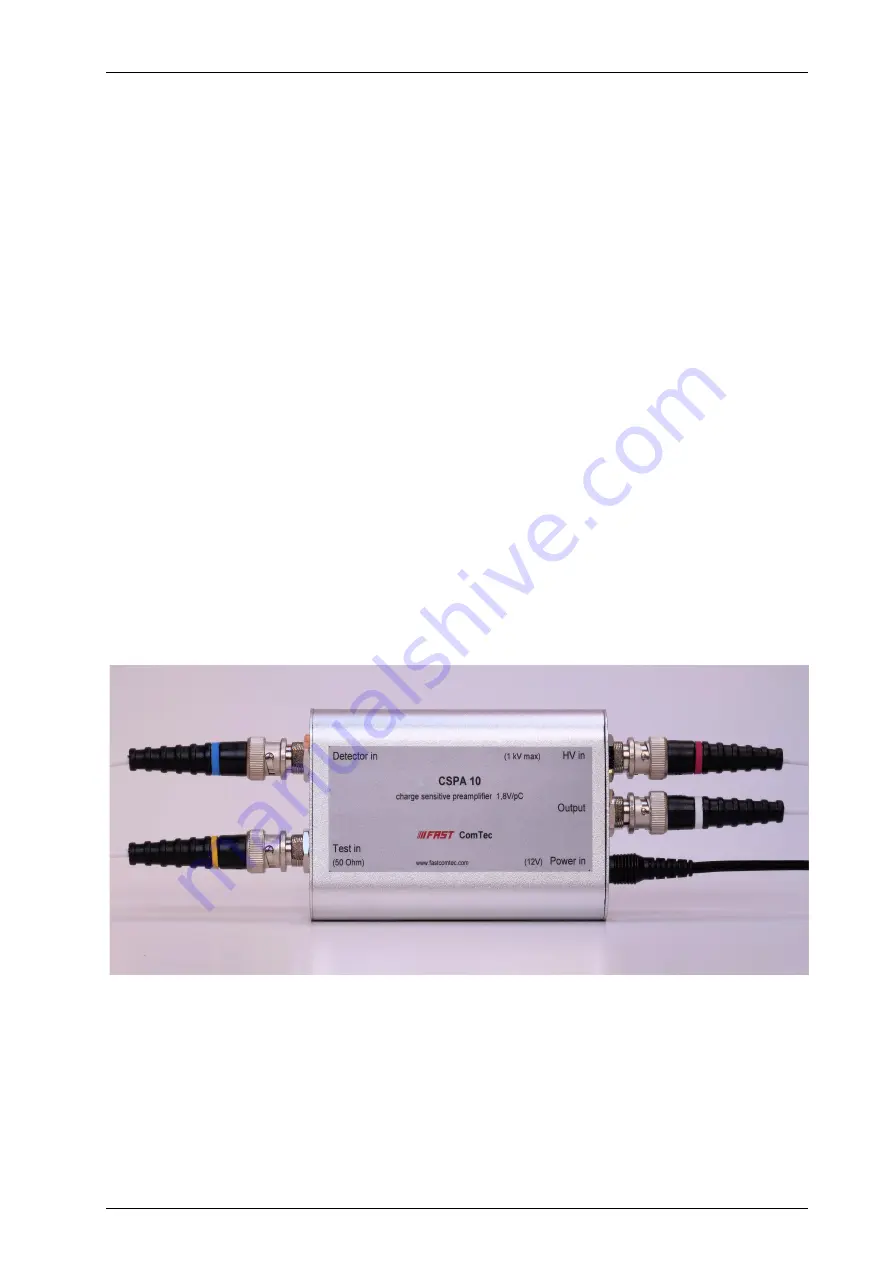
Page 12: ...controls and connectors located on the front and rear panels of the Model CSPA10 13 It is recommended that this section be read before proceeding with the operation of the preamplifier 3 2 Front Panel...
Page 13: ...the value of R reduced to provide a voltage drop The latter will cause the 0 pF noise of the preamplifier to increase but this will usually be insignificant compared to the noise generated in the det...
Page 14: ...tors This input does provide a resistive terminating impedance In the endless mode data acquisition is started only once e g by a software start i e asynchronously to the rest of the experiment Then a...
Page 15: ...ined are far different from what is expected it then becomes necessary to troubleshoot the system First observe the amplifier output on an oscilloscope at various time base and amplitude settings Is t...
Page 16: ...oad resistor dirty or moist detector input connector If RE and RD are acceptable but the live spectrum RS is not as good as expected the problem is probably in the detector bad detector poor charge co...
Page 17: ...ime of the charge sensitive preamplifier output will be at least that long The output waveform of the CSP10 13 using a capacitively coupled fast square wave pulser at the input is shown below to the l...
Page 18: ...Theory of Operation 16 F ComTec GmbH Fig 6 1 Simplified circuit diagram...
Page 19: ...otection network active 2 3 protection passive JP3 1 2 shorted inp ser resistor 0 Ohm 2 3 inp ser resistor 100 Ohm JP9 1 2 shorted output resistor 1 Ohm 2 3 output resistor 50 Ohm marked default setti...
Page 20: ...Appendix 8 Appendix 8 1 Detailed Schematic of the CSPA10 13 18 F ComTec GmbH Fig 8 1 Detailed circuit diagram of CSPA1X...
Page 21: ...Appendix 8 2 Personal Notes F ComTec GmbH 19...