background image

JP14-R-LP & JP14-Q-LP F

ALCOM

 GPS R

ECEIVERS

V

ERSION

 1.0.0

Ball

Name

I/O

Description

Level

26

TIMERSYNC

O

Control outputs. Do not use, leave it open.

CMOS

27

SPI_EN

I

Control-line for production test. Do not use, leave it open.

28

SPI_CLK

I

Control-lines   for   production   test.   Do   not   use,   leave   it 

open.

29

NADC_D

I

Do not use, leave it open.

30

SPI_DATA

O

Control-line for production test. Do not use, leave it open.

31

NSRESET

I

Do not use, leave it open.

CMOS

32

GND

33

GND

34

GND

Digital grounds

0 V

35

GND_RF

Analogue grounds

0 V

36

RF_IN

I

GPS signal from connected antenna

50 Ohms @ 1.575 GHz

37

NC

38

NC

39

NC

40

NC

-

Not connected

-

Table 2:

 Pin assignment of the JP14-Q

6.3 Configuration and timing signals

M-RST

This   pin   provides   an   active-low   reset   input   to   the  
board.   It   causes   the   board   to   reset   and   to   start 
searching   for   satellites.   If   not   utilized,   this   input   pin  
may be left open.

T-MARK

This pin provides 1 pulse per second output from the  
board, which is synchronized to within 1 microsecond 
of GPS time. The output is a CMOS level signal. 

BOOTSEL

Set this Pin to high (+3.3 V DC) for reprogramming the 
flash of the JP14-R-LP/Q-LP (for instance updating a 
new firmware for the JP14-R-LP/Q-LP).

6.4 Serial communication signals

The   board   supports   two   full   duplex   serial   channels.   All   serial   connections   are   at 
CMOS level. If you need different voltage levels, use appropriate level shifter, (e.g. 
MAX 3232 from Maxim) in order to obtain RS232 compatible signal levels (see also 
chapter   9).   All   supported   baud   rates   can   be   controlled   from   the   appropriate 
screens in SiRFdemo software. You can directly communicate with it through a PC 
serial port.

SDI1

This   is   the   main   receiving   channel   and   is   used   to 
receive   software   commands   to   the   board   from  
SiRFdemo software or from user written software.

SDI2

This is the auxiliary receiving channel and is used to  
input differential corrections to the board to enable  
DGPS   navigation.  

Note   that,   the   current   operating 

firmware does not support DGPS

.

SDO1

This is the main transmitting channel and is used to 
output   navigation   and   measurement   data   to 
SiRFdemo or user written software.

SDO2


For user’s application (It is not supported by default 
GSW3.1.0).

This confidential document is the property of FALCOM  and may not be copied or circulated without permission.

Page 21

Summary of Contents for JP14-Q-LP

Page 1: ...THIS DOCUMENT IS AVAILABLE AT HTTP WWW FALCOM DE JP14 R LP JP14 Q LP GPS Receivers Lead free products Hardware description Version 1 0 0 Created Monday 25 February 2008...

Page 2: ...DGPS Accuracy 13 5 3 1 4 Datum 13 5 3 1 5 Time to First Position 13 5 3 1 6 Sensitivity 14 5 3 1 7 Dynamic Conditions 14 5 3 1 8 DC Power 14 5 3 1 9 Serial Port 14 5 3 1 10 Time 1PPS Pulse 14 5 4 Pow...

Page 3: ...essages 24 7 2 3 Transport Message 25 8 MECHANICAL DRAW 26 9 LAYOUT RECOMMENDATION 29 9 1 Ground planes 29 9 2 RF connection 29 9 3 Soldering profile 30 10 FIRST STEPS TO MAKE IT WORK 31 11 APPENDIX 3...

Page 4: ...on history This table provides a summary of the document revisions Version Author Changes Release date 1 0 0 F Beqiri Initial version 25 02 2008 This confidential document is the property of FALCOM an...

Page 5: ...de Trademarks Some mentioned products are registered trademarks of their respective companies Copyright This document is copyrighted by FALCOM WIRELESS COMMUNICATIONS GmbH with all rights reserved No...

Page 6: ...ch unit has an integrated temperature compensated crystal oscillator TCXO Due to the higher stability of frequency they offer a high improved GPS performance In addition higher sensitivity allows them...

Page 7: ...breviations Abbreviation Description A GPS Assisted Global Positioning System BGA Ball Grid Array DGPS Differential GPS DOP Dilution of Precision GPS Global Positioning System GGA GPS Fixed Data LNA L...

Page 8: ...uit Board PRN Pseudo random noise IF Intermediate Frequency A D Analog Digital 1 3 Related documents 1 SiRF binary and NMEA protocol specification www falcom de Support Documentation Sirf SiRFmessages...

Page 9: ...s The GPS receiver consists of many small parts which can come loose and could be swallowed by small children Thoughtless handling can damage the GPS receiver 2 4 Operation antenna Operate the GPS rec...

Page 10: ...ns for the protection of public exposure to RF electromagnetic energy established by government bodies and professional organizations such as directives of the European Community Directorate General V...

Page 11: ...p 4 Mbit FLASH and 1 Mbit SRAM Operating voltage 3 3 V DC 5 Power consumption 140 mW continuous mode Power management Adaptive TricklePower ATP Push to Fix PTF For more details see chapter 5 4 Tempera...

Page 12: ...y make the JP14 R LP Q LP highly efficient engines for wide variety of location applications The core of JP14 R LP Q LP contains a built in sequencer which handles all the high rate interrupts for GPS...

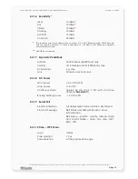
Page 13: ...6 12 5 25 and 49 MHz Data bus 16 bit 5 3 1 2 Accuracy Position Autonomous 10 meters CEP without SA SBAS 5 meter Velocity 0 1 meters second without SA Time 1 microsecond synchronized to GPS time 5 3 1...

Page 14: ...1000 knots max Acceleration 4 g max Jerk 20 meters second max 5 3 1 8 DC Power Main power 3 3 V DC 5 Core power 1 5 V DC Continuous mode approx 45 mA at 3 3 V DC with an active antenna FAL ANT 3 Backu...

Page 15: ...l be needed on the next power up scenario 5 4 2 Adaptive TricklePower mode ATP Adaptive TricklePower ATP is a variant of TricklePower But only ATP and Push To Fix PTF is described in next chapter mode...

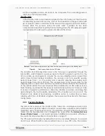
Page 16: ...to 900 ms The receiver turns to full power state for the sampling time to collect data and then operates in Standby state for the remainder of the update period The next full power state is initiated...

Page 17: ...messages to the target unit refer to chapter Appendix section 11 1 page 33 Syntax PSRF107 Mode OnTimeMs LPInterval MaxAcqTimeMs MaxOffTimeMs TPAdaptive CS CR LF Examples PSRF107 1 400 2000 60000 6000...

Page 18: ...target receiver should remain off sleep mode before making another attempt to navigate This mode is enabled if the target receiver is turned on and acquires satellites but does not navigate This mode...

Page 19: ...n 13 NC Not connected 14 NC 15 NC 16 GPIO0 I O General propose input output CMOS 17 NC Not connected 18 GND Digital ground 0 V 19 GND_RF Analogue ground 20 VANT I Power supply for an active antenna Up...

Page 20: ...t for baseband processor Do not use leave it open CMOS 10 PWRCTL O Control outputs Do not use leave it open CMOS 11 BOOTSEL I Boots the unit into the Update mode if it is set to HIGH CMOS VCC 12 WAKEU...

Page 21: ...t this Pin to high 3 3 V DC for reprogramming the flash of the JP14 R LP Q LP for instance updating a new firmware for the JP14 R LP Q LP 6 4 Serial communication signals The board supports two full d...

Page 22: ...a bias for an external active antenna can be provided in two ways to pin VANT In order to use a 5 V or 12 V active GPS antenna the VANT has to be connected to 5 V 12 V external power supply respective...

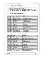
Page 23: ...E 30 Nav Lib SV State Data Satellite State Data 0 x 1F 31 Nav Lib Initialization Data Initialization Data 0 x FF 255 Development Data Various status messages Table 6 SiRF Output Messages Table 7 lists...

Page 24: ...umbers elevation azimuth and SNR values MSS This message can be switched on via SiRFdemo software Signal to noise ratio signal strength frequency and bit rate from a radio beacon receiver RMC Time dat...

Page 25: ...m the example strings but must be sent to terminate the message and cause the receiver to process that input message CheckSum The checksum is 15 bit checksum of the bytes in the payload data The follo...

Page 26: ...L The absolute maximum dimension of the modules are JP14 R 10 2 mm x 24 5 mm B x L and JP14 Q 15 7 mm x 17 2 mm B x L Figures 6 and 7 show the top view of the JP14 R LP Q LP GPS receivers and provide...

Page 27: ...soldering Figure 8 shows the bottom view on JP14 R and provides an overview of the mechanical dimensions of the pointed balls Figure 8 The mechanical draw of the JP14 R This confidential document is...

Page 28: ...hows the bottom view on JP14 Q and provides an overview of the mechanical dimensions of the pointed balls Figure 9 The mechanical draw of the JP14 Q This confidential document is the property of FALCO...

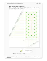
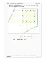
Page 29: ...re 10 Digital GND Analog GND connected internally Figure 10 Ground plane of the JP14 R LP Q LP GPS receivers 9 2 RF connection The JP14 R LP Q LP GPS receivers are designed to be functional by using e...

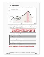
Page 30: ...is a reference to the soldering machine FALCOM utilizes This profile can vary by using different paste types and soldering machines and it should be adapted to the customer application NO liability is...

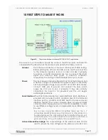
Page 31: ...ines which supply the VCC pin to 3 3 V properly If they are correctly connected the board is full powered and the unit begins obtaining its position fix Serial Interface The JP14 family provides two s...

Page 32: ...Evaluation board with connected JP14 R LP Q LP GPS receiver The GPS Evaluation Kit contains Evaluation Box JP14 sample with soldered antenna cable power supply AC DC adapter Type FW738 05 Output 5VDC...

Page 33: ...o do this open Action menu from main window and start Transmit Serial Message On the appeared dialog box select NMEA protocol from the Protocol Wrapper option and type the following command onto the m...

Reviews: