background image

APPLICATION NOTE

AN42

3


RC5040 and RC5042 Description

Simple Step-Down Converter

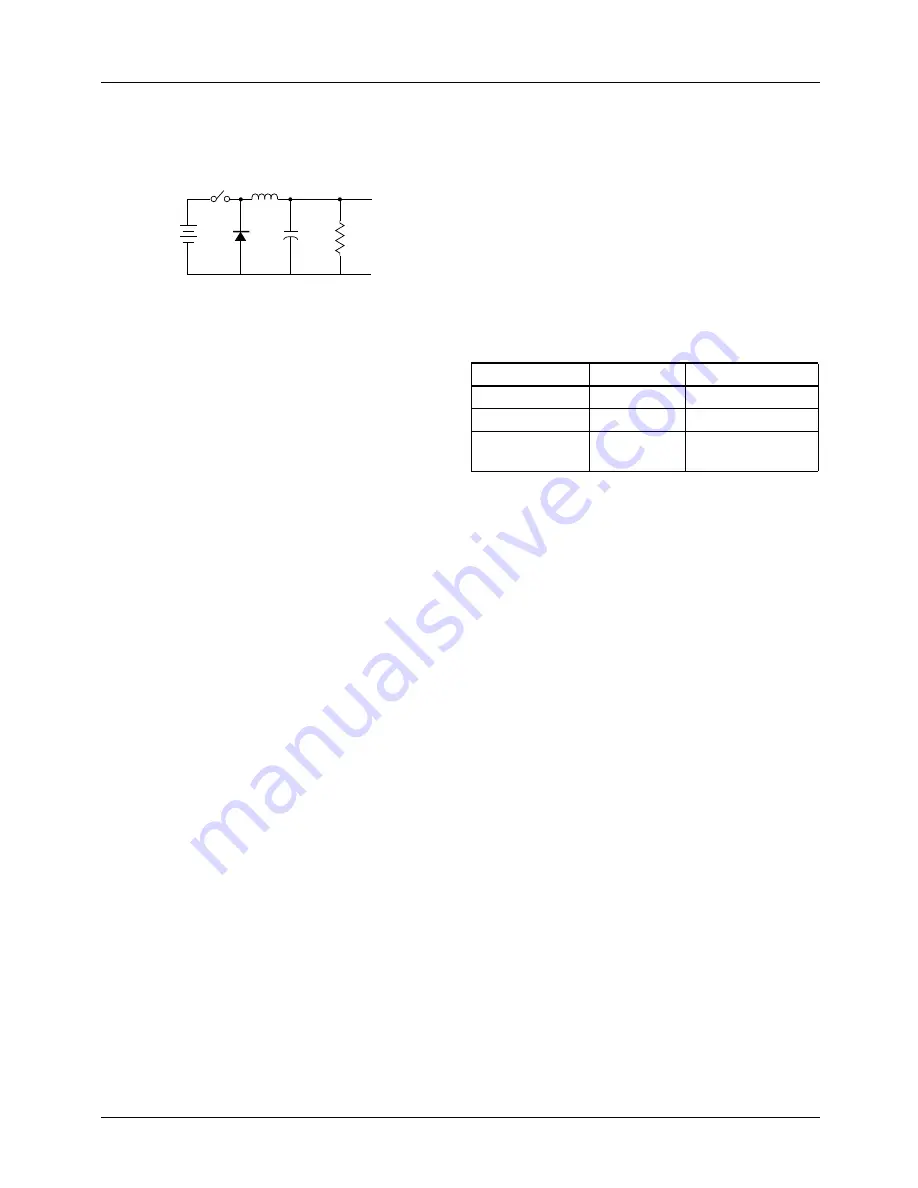
Figure 1. Simple Buck DC-DC Converter

Figure 1 illustrates a step-down DC-DC converter with no 
feedback control. The basic step-down converter serves as 
the basis for deriving the design equations for the RC5040 
and RC5042. From Figure 1, the basic operation begins by 
closing the switch S1, so that the input voltage V

IN

 is 

impressed across inductor L1. The current flowing through 
this inductor is given by the following equation:

where T

ON


is the duty cycle (the time when S1 is closed).

When S1 opens, the diode D1 conducts the inductor 
current and the output current is delivered to the load accord-
ing to the following equation:

where T

S

 is the overall switching period and (T

S

 – T

ON

) is 

the time during which S1 is open.

By solving these equations you can obtain the basic relation-
ship for the output voltage of a step-down converter:

In order to obtain a more accurate approximation for V

OUT

we must also include the forward voltage V

D

 across diode 

D1 and the switching loss, V

SW

. After taking into account 

these factors, the new relationship becomes:

Where V

SW

 = I

L

 • R

DS,ON

.

The RC5040 and RC5042 Controllers

The RC5040 is a programmable synchronous-mode DC-DC 
converter controller. The RC5042 is a non-synchronous ver-
sion of the RC5040. When designed with the appropriate 
external components, either device can be configured to 
deliver more than 14.5A of output current. During heavy 
loading conditions, these controllers function as current-
mode PWM step-down regulators. Under light loads, they 
function in PFM (pulse frequency modulation) or pulse skip-
ping mode. The controllers sense the load level and switch 
between the two operating modes automatically, thus opti-
mizing efficiency under all loads. The key differences 
between the RC5040 and RC5042 are listed in Table 4.

Table 4. RC5040 and RC5042 Differences

Refer to the RC5040 Block Diagram illustrated in Figure 2. 
The control loop of the regulator contains two main sections: 
the analog control block and the digital control block. The 
analog block consists of signal conditioning amplifiers feed-
ing into a set of comparators which provide the inputs to the 
digital block. The signal conditioning section accepts inputs 
from the IFB (current feedback) and VFB (voltage feedback) 
pins and sets two controlling signal paths. The voltage con-
trol path amplifies the VFB signal and presents the output to 
one of the summing amplifier inputs. The current control 
path takes the difference between the IFB and VFB and pre-
sents the result to another input of the summing amplifier. 
These two signals are then summed together with the slope 
compensation input from the oscillator. This output is then 
presented to a comparator, which provides the main PWM 
control signal to the digital control block.

The additional comparators in the analog control section sets 
the threshold for when the RC5040 enters PFM mode during 
light loads and the point when the current limit comparator 
disables the output drive signals to the MOSFETs.

The digital control block is designed to take the comparator 
inputs along with the main clock signal from the oscillator 
and provide the appropriate pulses to the HIDRV and 
LODRV pins that control the external power MOSFETs. The 
digital section was designed utilizing high speed Schottky 
transistor logic, thus allowing the RC5040 to operate at clock 
speeds as high as 1MHz. 

C1

R

L

 Vout

+

D1

V

IN

65-AP42-01

L1

S1

I

L

V

IN

V

OUT

(

)

T

ON

L1

-----------------------------------------------

=

I

L

V

OUT

T

S

T

ON

(

)

L1

--------------------------------------------

=

V

OUT

V

IN

T

ON

T

S

-----------

=

V

OUT

V

IN

V

D

V

SW

+

(

)

T

ON

T

S

-----------

V

D

=

RC5040

RC5042

Operation

Synchronous

Non-Synchronous

Package

20-pin SOIC

16-pin SOIC

Output Enable/ 
Disable

Yes

No

Summary of Contents for SEMICONDUCTOR RC5040

Page 1: ...In a high volume production envi ronment such as with personal computers however a CPU voltage change requires a CPU board re design to accommo date the new voltage requirement The integrated 4 bit D...

Page 2: ...r must be greater than 80 at high current draw and greater than 40 at low current draw Processor Voltage Identification The Pentium Pro package has four voltage identification pins VID3 VID0 that can...

Page 3: ...cally thus opti mizing efficiency under all loads The key differences between the RC5040 and RC5042 are listed in Table 4 Table 4 RC5040 and RC5042 Differences Refer to the RC5040 Block Diagram illust...

Page 4: ...0mV increments To guarantee stable operation under all loads a 10K pull up resistor and 0 1 F of decoupling capacitance should be connected to the VREF pin No load should be imposed on this pin Power...

Page 5: ...ripple current flowing through the output inductor allowing the use of a larger inductor value Operation at lower fre quencies increases the amount of energy storage that the bulk output capacitors mu...

Page 6: ...65 AP42 04 R7 10K C1 1000 F C2 C3 1000 F 1000 F C5 0 1 F DS2 1N5817 C12 1 F L1 1 3 H M1 2SK1388 M2 2SK1388 C8 C9 0 1 F 0 1 F RSENSE 8m 1500 F C13 L2 2 6 H M3 2SK1388 VREF C15 C14 1500 F 1500 F C4 0 1...

Page 7: ...5 TO 220 JA 62 5 NDP606AL TJ 125 C 33 40 JC 1 5 Motorola VGS 5V ID 37 5A TJ 25 C 6 9 TO 263 JA 62 5 MTB75N03HDL TJ 125 C 9 3 14 D2 PAK JC 1 0 Int Rectifier VGS 5V ID 31A TJ 25 C 28 TO 220 JA 62 5 IRLZ...

Page 8: ...re 7 illustrates how an external 12V source can be used to bias VCCQP A 47 resistor is used to limit the transient current into the VCCQP pin and a 1 F capacitor filter is used to filter the VCCQP sup...

Page 9: ...gate charge and f is the switching frequency Efficiency POUT pIN IOUT VOUT IOUT VOUT PLOSS PLOSS PDMOSFET PDINDUCTOR PDRSENSE PDGATE PDDIODE PDTRAN PDCAP PDIC 1 PDMOSFET IOUT 2 RDS ON DutyCycle DutyCy...

Page 10: ...rs This methodology limits the power delivered to the load during an overcurrent condition The voltage drop cre ated by the output current flowing across a sense resistor is presented to one terminal...

Page 11: ...037 0 5 1 650 10 3 1 048A RSENSE Vth min ISC 1 TF Vth min 1 0 ILoad max 1 TF Table 7 Comparison of Sense Resistors Refer to Appendix A for Directory of component suppliers Description Motherboard Tra...

Page 12: ...ue where R20 is the resistance at 20 C 20 0 00393 C T is the operating temperature andR is the desired value For temperature T 50 C the R change 12 Table 9 is a summary of tolerances for the Embedded...

Page 13: ...he output voltage as the load regulation col lapses into the short circuit control mode The output voltage does not return to its nominal value until the output short cir cuit current is reduced to wi...

Page 14: ...the Schottky diode is not being over stressed during a short circuit condition Schottky Diode Selection The application circuits of Figures 3 4 and 5 show two Schottky diodes DS1 and DS2 In synchronou...

Page 15: ...ity output voltage ripple and load transient response The calcu lation is as follows where V is the maximum voltage deviation due to load transients T is the reaction time of the power source and IO i...

Page 16: ...for the MOSFETs In general noisy switching lines should be kept away from the quiet analog section of the RC5040 That is traces that connect to pins 12 and 13 HIDRV and VCCQP should be kept far away...

Page 17: ...le and Silk Screen are presented below The actual PCAD Gerber File can be obtained from Raytheon Electronics Semicon ductor Division s Marketing Department at 415 966 7819 Figure 16 Example of Proper...

Page 18: ...AN42 APPLICATION NOTE 18...

Page 19: ...d at 1A increments an active load HP6060B or equivalent is suggested 6 In case of poor regulation refer to the procedures in the Troubleshooting section Troubleshooting 1 If no voltage is registered a...

Page 20: ...overshoots then the noise may cause the converter to function improperly 9 Next look at the HIDRV pin This pin directly drives the gate of the FET It should provide a gate drive Vgs of about 5V when t...

Page 21: ...th the supply However with the input filter design the Input Rush Current will be well within specification VID Iload A Vout V 1010 0 5 2 505 1 0 2 504 2 0 2 501 3 0 2 496 4 0 2 493 5 0 2 493 6 0 2 49...

Page 22: ...evice Description Case Temperature C Iload 9 9A Case Temperature C Iload 12 4A Case Temperature C Iload 13 9A Q3A MOSFET K1388 57 63 56 3 Q3B MOSFET K1388 58 64 66 6 L1 Inductor Unknown 53 56 61 2 Q2...

Page 23: ...design considerationsn and component selec tions layout guidelines and considerations guidelines for debugging and performance evaluations RC5040 RC5042 Evaluation Board Raytheon Electronics provides...

Page 24: ...00 Fax 852 2314 0061 National Semiconductor Japan Ltd Tel 81 3 5620 6175 Fax 81 3 5620 6179 Appendix A Directory of Component Suppliers Dale Electronics Inc E Hwy 50 PO Box 180 Yankton SD 57078 0180 P...

Reviews: