ISPJUNO - Portable ISP Programmer - User Guide V0.84 – 17/04/20
38
5.6 Target ISP Port – 16-way connector pin-out
The
‘Target ISP Connector’
port features all the signals required to implement In-System
Programming (ISP) of a Target IC using the SPI, JTAG, I2C, XMEGA PDI, ATtiny TPI or UART
interface. This connector also features the programmable
“Target Vcc”
and
“Target Vpp”
voltages
plus a switched
“EXTERNAL Vcc”
supply.
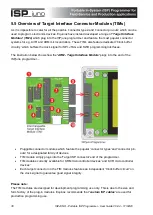
The illustration below shows the location of the
‘Target ISP Connector’
port on the rear panel of the
programmer.
‘Target ISP Connector’
port
The connector is a 16-pin bump-polarised IDC
connector with 0.1” pin spacing.
Pin 1 is the top right pin as shown in the diagram
opposite.
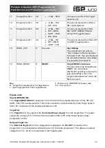
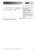
The pin-out of this connector is detailed in the table below.
Pin
No
Programmer
Pin name
I/O
Connect to pin on
Target System
Notes
1 + 2
TARGET_VCC
P
TARGET_VCC
Target VCC
This pin should be connected to the
Target System Vcc.
3 + 4
TARGET_EXT_VCC P
See notes.
Target External VCC
This pin should be connected to the
Target System Vcc.
Only use this pin if the
“External
Target Vcc”
is to be switched to
the
“Target Vcc”
5 + 6
PROG_GND
P
Signal GROUND (0V)
Signal Ground Connection (1)
0V to which the programmer JTAG,
SPI, I2C signal lines are referenced
to.
7a
7b
7c
I2C_SCL
XMEGA_PDI_CLK
ATTINY_TPI_CLK
I/O
O
O
•
I2C SCL
•
RESET
•
TPI_CLK
•
I2C SCL clock signal
•
XMEGA CLOCK Signal
•
ATtiny CLOCK Signal
8a
8b
8c
I2C_SDA
XMEGA_PDI_DATA
ATTINY_TPI_DATA
I/O
I/O
I/O
•
I2C SDA
•
TEST (PDI_DATA)
•
TPI_DATA
•
I2C SDA data signal
•
XMEGA DATA Signal
•
ATtiny DATA Signal
9
OP6
O
Algorithm specific
Spare Output
10
Programmer I/O5
I/O
•
Spare I/O


