1. Overview
2
Seiko Epson Corporation
S5U1C17564T Manual
(Rev.1.0)
1.1
Using the board
Follow the steps below to set up an evaluation environment to debug software for S1C17564 along with the
2”EPD panel from PDI.
<When you debug software>
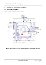
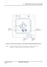
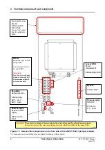
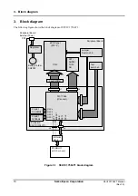
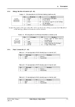
(1) Use the dedicated cables bundled with S5U1C17001H2 (ICDminiVer.2) to connect the 4-pin connector for
target connection and the 4-pin connector for power supply for Flash writing on the ICDminiVer.2 to the
connectors CN2-1(J5) and CN2-2(J6) on the CPU board respectively.
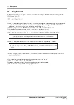
(2) Set the jumper switch for REGEN selection (JP2) on the CPU board to the
“
EN” side.
(3) Short-circuit the jumper switches JP1, JP5, JP6, and JP7 on the CPU board.
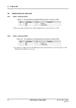
(4) You do not need to supply power for the power connectors JP7, JP8, and JP9 on the CPU board.
(5) Use the USB cable bundled with the ICDminiVer.2 to connect the ICDminiVer.2 to the PC.
<In the case of free running operation using a coin buttery (when the CPU board and the peripheral board are
used in combination.)>
(1) You do not need to change the jumper switch settings on the CPU board.
(2) Disconnect all the cables to the ICDminiVer.2.
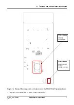
(3) Install a coin battery to the battery holder mounted on the peripheral board.
(4) Short-circuit the jumper (SW3) on the peripheral board.
*) Supply the power from the peripheral board (SVT17564: S5U1C17564T11).
*) As for the dip switch settings of the ICDminiVer.2, turn OFF all SW1-7 and turn ON
SW8.

