background image

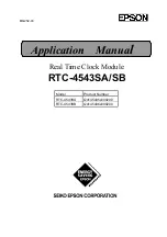
RTC - 4543 SA/SB


Page - 1 

MQ - 252 - 03


32-kHz Output Serial RTC Module 

RTC - 4543 SA/SB 


z

Built-in crystal permits operation without requiring adjustment


z

Built-in time counters (seconds, minutes, hours) and calendar counters (days, days of the week 

months, years)


z

Operating voltage range: 2.5 V to 5.5 V


z

Supply voltage detection voltage: 1.7 

±

0.3 V


z

Low current consumption: 1.0 

µ

A/2.0 V (Max.)


z

Automatic processing for leap years


z

Output selectable between 32.768 kHz/1 Hz


1. Overview 


This module is a real-time clock with a serial interface and a built-in crystal oscillator. This module 
is also equipped with clock and calendar circuits, an automatic leap year compensation function, 
and a supply voltage detection function. 
In addition, this module has a 32.768 kHz/1 Hz selectable output function for hardware control that 
is independent of the RTC circuit. 
This module is available in a compact SOP 14-pin package (RTC-4543SA) and a thin SOP 18-pin 
package (RTC-4543SB).


2. Block diagram 


OSC 

FOUT 

I / O 

CONTROLLER 

SHIFT REGISTER 

C

L

DATA 

CE 

WR 

32.768 kHz 

DIVIDER 

OUTPUT 

CONTROLLER 

FOE 

CONTROL 

CIRCUIT 

FSEL 

VOLTAGE 

 DETECT 

CLOCK  AND  CALENDAR 


Summary of Contents for RTC-4543SA

Page 1: ...MQ252 03 Application Manual Real Time Clock Module RTC 4543SA SB Model Product Number RTC 4543SA Q4145435x000200 RTC 4543SB Q4145436x000200 ...

Page 2: ...cence from the Ministry of International Trade and industry or other approval from another government agency The products except for some product for automotive applications listed up on this material are designed to be used with ordinary electronic equipment OA equipment AV equipment communications equipment measuring instruments etc Seiko Epson does not assume any liability for the case using th...

Page 3: ...4 DC CHARACTERISTICS 3 5 5 AC CHARACTERISTICS 4 5 6 TIMING CHARTS 5 6 TIMER DATA ORGANIZATION 6 7 DESCRIPTION OF OPERATION 7 7 1 DATA READS 7 7 2 DATA WRITES 7 7 3 DATA WRITES DIVIDER RESET 8 7 4 FOUT OUTPUT AND 1 HZ CARRIES 8 8 EXAMPLES OF EXTERNAL CIRCUITS 9 9 EXTERNAL DIMENSIONS 10 10 LAYOUT OF PACKAGE MARKINGS 10 11 REFERENCE DATA 11 12 APPLICATION NOTES 12 12 1 NOTES ON HANDLING 12 12 2 NOTES...

Page 4: ...Hz 1 Overview This module is a real time clock with a serial interface and a built in crystal oscillator This module is also equipped with clock and calendar circuits an automatic leap year compensation function and a supply voltage detection function In addition this module has a 32 768 kHz 1 Hz selectable output function for hardware control that is independent of the RTC circuit This module is ...

Page 5: ...A pin input output switching pin High DATA input when writing the RTC Low DATA output when reading the RTC FOE 6 5 Input When high the frequency selected by the FSEL pin is output from the FOUT pin When low the FOUT pin goes to high impedance VDD 9 14 Connects to positive side of the power supply CLK 10 12 Input Serial clock input pin Data is gotten at the rising edge during a write and data is ou...

Page 6: ...Monthly deviation Approx 1 min 5 4 DC Characteristics Unless specified otherwise VDD 5 V 10 Ta 40 to 85 C Item Symbol Conditions Min Typ Max Unit Current consumption 1 IDD1 VDD 5 0 V CE L FOE L 1 5 3 0 µA Current consumption 2 IDD2 VDD 3 0 V FSEL H 1 0 2 0 µA Current consumption 3 IDD3 VDD 2 0 V 0 5 1 0 µA Current consumption 4 IDD4 VDD 5 0 V CE L FOE H 4 0 10 0 µA Current consumption 5 IDD5 VDD 3...

Page 7: ...900 µs CE hold time tCEH 0 375 0 75 µs CE enable time tCE 0 9 0 9 s Write data setup time tSD 0 1 0 2 µs Write data hold time tHD 0 1 0 1 µs WR setup time tWRS 100 100 ns WR hold time tWRH 100 100 ns DATA output delay time tDATD 0 2 0 4 µs DATA output floating time tDZ 0 1 0 2 µs Clock input rise time tr1 50 100 ns Clock input fall time tf1 50 100 ns FOUT rise time CL 30 pF tr2 100 200 ns FOUT fal...

Page 8: ... tCES tCLK DATA tCLKH tCLKL tDATD tWRH tCEH tDZ tRCV tCE tCLKS 2 Data write WR tWRS CE t t f1 r1 CLK tCES tCLK DATA tCLKH tCLKL tWRH tCEH tSD tHD tRCV tCE tCLKS 3 FOUT output FOUT t tr2 10 90 50 tf2 tH Duty t t 100 H 4 Disable enable FOE VIH FOUT VIL tXZ tZX Disable High impedance Enable ...

Page 9: ...10 mo8 mo4 mo2 mo1 Year 0 to 99 y80 y40 y20 y10 y8 y4 y2 y1 bits Any data may be written to these bits FDT bit Supply voltage detection bit This bit is set to 1 when voltage of 1 7 0 3 V or less is detected between VDD and GND The FDT bit is cleared if all of the digits up to the year digits are read Although this bit can be both read and written normally set this bit to 0 Detection pulse VDD Mode...

Page 10: ...rror of 1 second 7 Complete data read operations within tCE Max 0 9 seconds as described earlier 7 2 Data writes CLK WR DATA 0 s40 s20 s10 s8 s4 s2 s1 y8 y10 y20 y40 CE y80 1 52 FDT 2 53 54 54 n Seconds Year 1 When the WR pin is high and the CE pin is high the RTC enters data input mode 2 In this mode data is input in succession and in synchronization with the rising edge of the CLK signal to the ...

Page 11: ...in tCE Max 0 9 seconds as described earlier 7 4 FOUT output and 1 Hz carries CLK WR CE 1Hz FOUT CLK t CES t 1 0 s 0 7 8 ms 15 6 ms 15 6 ms During a data write operation because a reset is applied to the Devider counter from the 128 Hz level to the 1 Hz level after the CE pin goes high during the time between the falling edge of the first clock cycle and the rising edge of the second clock cycle th...

Page 12: ...UT FSEL WR DATA CLK FOE VDD VDD Power supply Detection circuit Power supply Switching circuit 1 2 1 FOUT output frequency setting High 1 Hz low 32 768 kHz 2 Prohibits FOUT output during back up reducing current consumption Example 2 When used as a clock source oscillator RTC 4543 VDD CE GND 0 1 µF FOUT FSEL WR DATA CLK FOE VDD VDD VDD 1 ...

Page 13: ...B SOP 18pin 7 8 0 2 5 4 11 4 0 2 1 27 0 4 1 8 2 0 0 12 0 1 Max 0 Min 0 15 0 6 0 2 0 10 10 Layout of Package Markings RTC 4543 SA SOP 14pin R4543 E 1234A Model Manufacturing Lot B Frequency torerance RTC 4543 SB SOP 18pin R4543 E 1234A Model Manufacturing Lot B Frequency tolerance Note The markings and their positions as pictured above are only approximations These illustrations do not define the d...

Page 14: ...o determine the clock accuracy add in the frequency tolerance and the voltage characteristics f f f f0 fT fv f Clock accuracy at any given temperature and voltage frequency stability Frequency accuracy T v Frequency deviation at any given temperature Frequency deviation at any given voltage f f f0 f f 3 Determining the daily error Daily error f f 86400 seconds With error of 11 574 10 6 the error o...

Page 15: ...e pull up or pull down resistors should be provided for all unused input pins 12 2 Notes on packaging 1 Soldering heat resistance If the temperature within the package exceeds 260 the characteristics of the crystal oscillator will be degraded and it may be damaged The reflow conditions within our reflow profile is recommended Therefore always check the mounting temperature and time before mounting...

Page 16: ...915 Les Conquérants 1 Avenue de l Atlantique Z A de Courtaboeuf 2 91976 Les Ulis Cedex France Phone 33 0 1 64862350 Fax 33 0 1 64862355 ASIA EPSON CHINA CO LTD 23F Beijing Silver Tower 2 North RD DongSangHuan ChaoYang District Beijing China Phone 86 10 6410 6655 Fax 86 10 6410 7319 http www epson com cn 4F Bldg 27 No 69 Gui Qing Road Cao hejing Shanghai China Phone 86 21 6485 0835 Fax 86 21 6485 0...

Reviews: