


CARD-PCI/GX Hardware Manual
Rev.A
EPSON
77
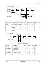
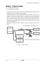
A.4.2 Address bus and data bus
The address and data busses, such as AD0-31 of PCI, SD0-15 and SA0-19 of ISA, should
be grouped by bus type for wiring. (Do not mix with other signals.) To avoid crosstalk,
do not wire these busses and other signals in parallel. If wiring in parallel, put GND
between the signals and busses.
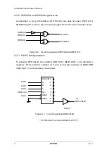
Other signal pattern
GND pattern
GND via
GND via
Bus signal pattern
A.4.3 PCI signal
Avoid making the PCI signal wiring too long since the PCI signal speed is higher than
those of ISA. If long wiring cannot be avoided or load is heavy, be sure to confirm the
waveform.
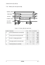
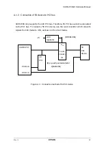
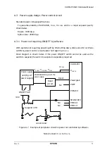
A.4.4 Clock signal
High speed clock signal are likely to negatively affect other signals by crosstalk or be
affected by other signals, resulting in trouble. To avoid such troubles, guard it using
GND patter as shown below.
GND via
Signal via
Clock signal
GND via
GND via
GND via
signal via
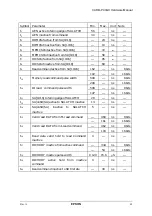
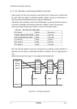
Clock signals requiring attention is shown below.
Clock signal name
Frequency
PCICLK0-2
33MHz
FPDOTCLK
25MHz
∼
65MHz
FPDOTE
12.5MHz
∼
32.5MHz
AC97BITCLK
12.288MHz (varies depending on Codec specifications)


