


nization circuit, which may drive a clock generated by the MPSoC device to all the DC/DC converters.
This feature can be controlled from the MPSoC device via two pins. Table 15 presents the control signals for
the power converter synchronization.
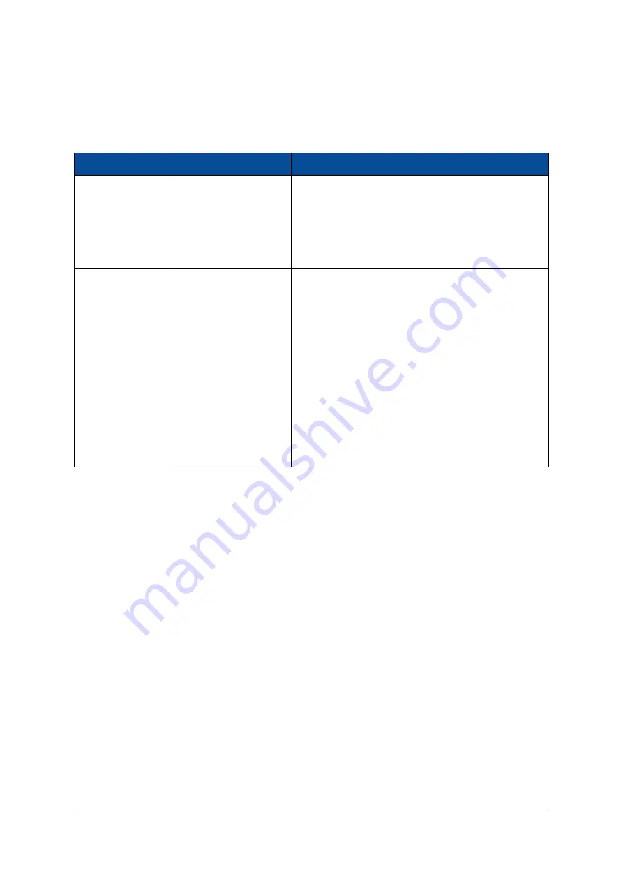
Signal
MPSoC Pin
Description
PWR_SYNC_EN#
MIO7 (package pin A18)
Enable signal for the power synchronization circuit. This
pin is equipped with a pull-up resistor to 1.8 V.
Drive this signal low to activate synchronization.
Leave this pin floating or drive it high to use the default
switching frequencies as specified in the schematics.
LED2#_PWR_SYNC
Package pin AE8
Multi-function FPGA pin.
When PWR_SYNC_EN# is low:
•
LED2#_PWR_SYNC floating/driven high: default
switching frequency (as specified in the schemat-
ics) is used.
•
LED2#_PWR_SYNC driven low:
invalid
, may
cause instability of all DC/DC converters on board.
•
LED2#_PWR_SYNC as clock signal: the DC/DC
converters are synchronized with this external
clock signal.
When PWR_SYNC_EN# is high (default configuration),
this pin is connected to LED2#.
Table 15: Power Converter Synchronization
The synchronization frequency valid for all switching DC/DC converters on-board and compensation net-
works must lie in the range 860..1000 kHz.
Depending on the selected frequency, it is recommended to adjust the duty cycle of the synchronization
clock accordingly, in order to ensure a minimum time of 600 ns for the high level of the clock signal. This
implies that for higher clock frequencies the duty cycle must be increased to 65-75%.
When VCC_IO_B65 is 1.0 V, the synchronization of the DC/DC converters to a user frequency is not supported,
as there is no 1.0 V output standard available in HP banks. For details on I/O standards, refer to the Zynq
Ult MPSoC, DC and AC Switching Characteristics [21].
2.11.2
Power Enable/Power Good
The XU1 SoC module provides a power enable input on the module connector. This input may
be used to shut down the DC/DC converters and LDOs for 0.72/0.85/0.9 V, 0.85/0.9 V, 0.9 V, 1.2 V, 1.8 V and
2.5 V. The list of regulators that can be disabled via PWR_EN signal is provided in Section 2.11.1.
The PWR_EN input is pulled to VCC_3V3 on the XU1 SoC module with a 10 k
Ω
resistor. The
PWR_GOOD signal is pulled to VCC_3V3 on the XU1 SoC module with a 10 k
Ω
resistor.
PWR_GOOD is an open collector signal and must not be used to drive a load directly. This signal is pulled
to GND if the on-board regulators fail or if the module is disabled via PWR_EN. The list of regulators that
influence the state of PWR_GOOD signal is provided in Section 2.11.1.
D-0000-428-001
32 / 66
Version 13, 15.08.2019


