Ebyte E01 Series User Manual Download Page 18

nRF24L01P wireless module

E01 series user manual

Copyright ©2012–2017,Chengdu Ebyte Electronic Technology Co.,Ltd.

17

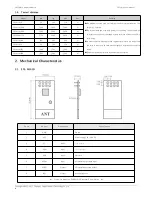
take measures such as shielding to reduce the influence of harmonic interference and inter-modulation interference.

[Crystal] If there is a crystal near the circuit board on the module, increase the linear distance between the crystal and circuit board as much as

possible.

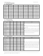
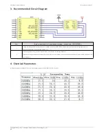
7. Production Guidance

7.1. Reflow Soldering Temperature
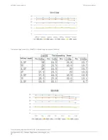
Profile Feature

Curve characteristics

Sn-Pb Assembly

Pb-Free Assembly

Solder Paste

Solder paste

Sn63/Pb37

Sn96.5/Ag3/Cu0.5

Preheat Temperature min (Tsmin)

Mini. preheating temperature

100℃

150℃

Preheat temperature max (Tsmax)

Max. preheating temperature

150℃

200℃

Preheat Time (Tsmin to Tsmax)(ts)

Preheating time

60-120 sec

60-120 sec

Average ramp-up rate(Tsmax to Tp)

Average rising rate

3℃/second max

3℃/second max

Liquidous Temperature (TL)

Liquidus temperature

183℃

217℃

Time(tL)Maintained Above(TL)

The time above the liquidus

60-90 sec

30-90 sec

Peak temperature(Tp)

Peak temperature

220-235℃

230-250℃

Aveage ramp-down rate(Tp to Tsmax)

Average rate of decline

6℃/second max

6℃/second max

Time 25℃ to peak temperature

The time from 25℃ to peak temperature

6 minutes max

8 minutes max

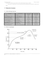
7.2. Reflow Curving Diagram

Summary of Contents for E01 Series

Page 1: ...Module E01 Series This manual may be modified based on product upgrade please refer to the latest version All rights to interpret and modify this manual belong to Chengdu Ebyte Electronic Technology...

Page 2: ...built in PA and LNA the 20dBm module has better performance for communication and operating range 0dBm modules with imported parts owns excellent RF performance especially popular among users who req...

Page 3: ...wer 5 1 3 2 Receiving sensitivity 5 1 3 3 Recommended operating frequency 5 1 4 Tested distance 6 2 Mechanical Characteristics 6 2 1 E01 ML01D 6 2 2 E01 ML01DP4 7 2 3 E01 ML01DP5 8 2 4 E01 2G4M27D 9 2...

Page 4: ...odule The current at the instant of transmitting may be high but the total energy consumed may be lower due to very short transmitting time When using external antenna the impedance matching degree at...

Page 5: ...al pulse is higher than the maximum power supply voltage The power supply is not advisable to be below 3 0V or the RF parameters will be influenced at different degree For max 30dBm voltage is no less...

Page 6: ...1 ML01D 92 0 93 0 94 0 dBm The sensitivity is tested under the air data rate 250kbps Due to the error of the materials each LRC component has 0 1 error so error accumulation will occur since multiple...

Page 7: ...tests in clear air with little electromagnetic interference at suburb areas Distance may be shorter with interference or obstacles E01 ML01DP4 1600 1800 1980 m E01 ML01DP5 2300 2500 2800 m E01 2G4M27...

Page 8: ...plication 1 GND Ground connect to power reference ground 2 VCC Power supply 2 0 V 3 6V DC 3 CE input Chip enable 4 CSN input SPI Chip select 5 SCK input SPI Clock 6 MOSI input SPI master output slave...

Page 9: ...direction Pin application 1 GND Ground 2 VCC Power supply 2 0V 3 6V DC 3 CE input Chip enable 4 CSN input SPI Chip select 5 SCK input SPI Clock 6 MOSI input SPI master output slave input 7 MISO Outpu...

Page 10: ...application 1 GND Ground 2 VCC Power supply 2 5V 5 5V DC it s recommended to use 3 3V 3 CE input Chip enable 4 CSN input SPI Chip select 5 SCK input SPI Clock 6 MOSI input SPI master output slave inp...

Page 11: ...n direction Pin application 1 VCC Power supply 1 9V 3 6V DC 2 CE Input Chip enable 3 CSN Input SPI Chip select 4 SCK Input SPI Clock 5 MOSI Input SPI master output slave input 6 MISO Output SPI master...

Page 12: ...direction Pin application 1 VCC Power supply 1 9V 3 6V DC 2 CE Input Chip enable 3 CSN Input SPI Chip select 4 SCK Input SPI Clock 5 MOSI Input SPI master output slave input 6 MISO Output SPI master...

Page 13: ...n application 1 VCC Power supply 2 0 V 3 6V DC 2 CE Input Chip enable 3 CSN Input SPI Chip select 4 SCK Input SPI Clock 5 MOSI Input SPI master output slave input 6 MISO Output SPI master input slave...

Page 14: ...n application 1 VCC Power supply 2 0 V 3 6V DC 2 CE Input Chip enable 3 CSN Input SPI Chip select 4 SCK Input SPI Clock 5 MOSI Input SPI master output slave input 6 MISO Output SPI master input slave...

Page 15: ...ds to set as POWER DOWN mode when the module writes registers and it is recommended that CE is controlled by MCU pin 2 As interrupt pin for IRQ it can be used to wake up MCU and achieve fast response...

Page 16: ...user manual Copyright 2012 2017 Chengdu Ebyte Electronic Technology Co Ltd 15 The real transmitting power of E01 2G4M27D in different voltage testing under 2460MHz The corresponding register value of...

Page 17: ...supply has a great influence on the performance of the module Make sure that the power supply of the module has a small ripple and you must avoid large power jitter It is recommended to use type filte...

Page 18: ...r Paste Solder paste Sn63 Pb37 Sn96 5 Ag3 Cu0 5 Preheat Temperature min Tsmin Mini preheating temperature 100 150 Preheat temperature max Tsmax Max preheating temperature 150 200 Preheat Time Tsmin to...

Page 19: ...power Due to antenna quality or poor matching between antenna and module 8 2 Module is easy to damage Please check the power supply source ensure it is within the recommended value voltage higher tha...

Reviews: