U
SER
M
ANUAL
16
K
/8
K
CXP
C
OLOR
–
R
EV
G
–
09/2016
P
A G E
|
23
7.2.1
Structure of the Sensor
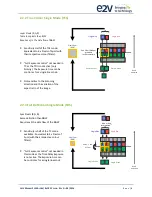
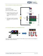
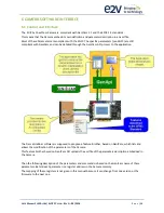
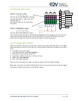
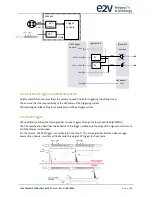
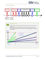
Pixels in « True Color » modes :
P
n
=
R
(n)
,
G
B(n)
,
B
(n)
Each Pixel has to be considered as a 10x10µm
pixel including 2 1xRed and 1x Blue,
all Pixels of 5x5µm.
The Enhanced mode has the double of this
information
Pixels in « Full Definition » modes :
P
n
=
R
(n-1)
,
G
B(n)
,
B
(n)
P
n+1
=
R
(n+1)
,
G
R(n+1)
,
B
(n)
Each pixel has to be considered as a 5x5µm
pixels. The Red or Blue information is alternatively interpolated from the neighbour pixel. The Enhanced
mode has the double of this information : In this mode, the sensor works in TDI Mode and requires a
specific mode (“Full Exposure Control”) when the User wants to control the exposure
7.2.2
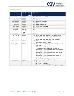
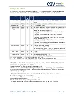
Test Image Pattern Selector
This selection
Defines if the data comes from the normal Sensor operation and FPGA Chain or from digital
patterns generated at the end of the FPGA. This is mainly useful to detect some interfacing or connection
issues.
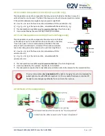
To switch to Cmos sensor image
Grey Horizontal Ramp (Fixed) :
See AppendixA
White Pattern (Uniform white image : 255)
Grey Pattern (Uniform middle Grey : 128 on each color)
RGBW Pattern
See AppendixA
Grey vertical Ramp (moving)
When any of the Test pattern is enabled, the whole processing chain of the FPGA is disabled.
Note
: When the camera is set with the RGBW pattern test, it’s no more taking in account the Line Trigger
and working in Free Run (line period controlled by the camera)
ADC
ADC
Memory node
Pixel Line A
Pixel Line B
Pixel Line C
Pixel Line D
Memory node
Green
«
Blue
»
Pixels (
G
B
)
Green
«
Red
»
Pixels (
G
R
)
G
B
G
B
G
B
G
R
G
R
G
R
P
n-1
P
n-1
P
n
P
n+1
P
n+2
P
n+3
P
n-1
P
n
P
n+1

