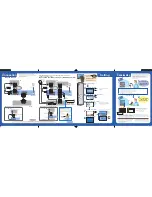
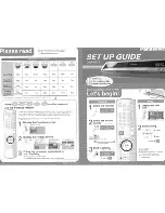
background image

1-12-6

E9B05SCM4

Main 4/9 Schematic Diagram  < VCR Section >

www.freeservicemanuals.info

18/6/2013

World of free manuals

Summary of Contents for ADB2737BD

Page 1: ...ications I Preparation for Servicing I Adjustment Procedures I Schematic Diagrams I CBA s I Exploded views I Parts List When servicing the deck mechanism refer to MK14 Deck Mechanism Section Deck Mechanism Part No N25E0FL PAL www freeservicemanuals info 18 6 2013 World of free manuals ...

Page 2: ...0 1 Block Diagrams 1 11 1 Schematic Diagrams CBA s and Test Points 1 12 1 Waveforms 1 13 1 Wiring Diagram VCR Section 1 14 1 Wiring Diagram DVD Section 1 14 2 IC Pin Function Descriptions 1 15 1 Lead Identifications 1 16 1 Exploded Views 1 17 1 Mechanical Parts List 1 18 1 Electrical Parts List 1 19 1 Main Section I Specifications I Preparation for Servicing I Adjustment Procedures I Schematic Dia...

Page 3: ... N AM R P dB 37 41 SP Mode 1 5 Video Color S N PM R P dB 30 36 SP Mode 1 6 Resolution PB Line 230 245 SP Mode 2 Servo 2 1 Jitter Low µsec 0 07 0 12 SP Mode 2 2 Wow Flutter 0 3 0 5 SP Mode 3 Normal Audio 3 1 Output PB dBV 9 4 3 SP Mode 3 2 Output R P dBV 9 4 1 5 SP Mode 3 3 S N R P dB 36 41 SP Mode 3 4 Distortion R P 1 0 4 0 SP Mode 3 5 Freq resp R P at 200Hz dB 6 2 SP Mode 20dB ref 1kHz at 8kHz dB...

Page 4: ...75 Ω load Vp p 0 3 2 AUDIO 2 1 Output Level Vrms 2 0 2 2 Frequency Response DVD VIDEO LPCM fs 96 kHz Hz 20 44 k fs 48 kHz Hz 20 20 k Audio CD fs 44 1 kHz Hz 20 20 k 2 3 Signal Noise Ratio DVD VIDEO LPCM dB 85 CD dB 85 REC Playback Input 2 Vrms Rec Speed SP dB 85 2 4 THD N 1 kHz 0 dB DVD VIDEO LPCM 0 01 CD 0 01 REC Playback Input 2 Vrms Rec Speed SP 0 01 3 TUNER 3 1 Video Output 75 Ω load Vp p 1 0 ...

Page 5: ...he diode is turned on Do not look directly at the laser beam CAUTION Use of controls and adjustments or doing procedures other than those specified herein may result in hazardous radiation exposure Location Inside Top of DVD mechanism Do not look directly at the laser beam coming from the pickup or allow it to strike against your skin Drive Mechanism Assembly Laser Beam Radiation Laser Pickup Turn...

Page 6: ...ith part number specified B In addition to safety other parts and assemblies are specified for conformance with regulations applying to spurious radiation These must also be replaced only with specified replacements Examples RF converters RF cables noise block ing capacitors and noise blocking filters etc C Use specified internal wiring Note especially 1 Wires covered with PVC tubing 2 Double insu...

Page 7: ...m the specified or lower leakage current between B earth ground power cord plug prongs and externally exposed accessible parts RF termi nals antenna terminals video and audio input and output terminals microphone jacks earphone jacks etc is lower than or equal to the specified value in the table below Measuring Method Power ON Insert load Z between B earth ground power cord plug prongs and exposed...

Page 8: ...the Flat Pack IC about 5 to 6 seconds Fig S 1 1 2 Remove the flat pack IC with tweezers while apply ing the hot air 3 Bottom of the flat pack IC is fixed with glue to the CBA when removing entire flat pack IC first apply soldering iron to center of the flat pack IC and heat up Then remove glue will be melted Fig S 1 6 4 Release the flat pack IC from the CBA using twee zers Fig S 1 6 Caution 1 The ...

Page 9: ...first apply soldering iron to center of the flat pack IC and heat up Then remove glue will be melted Fig S 1 6 4 Release the flat pack IC from the CBA using twee zers Fig S 1 6 With Iron Wire 1 Using desoldering braid remove the solder from all pins of the flat pack IC When you use solder flux which is applied to all pins of the flat pack IC you can remove it easily Fig S 1 3 2 Affix the wire to a...

Page 10: ...ing braid remove the solder from the foil of each pin of the flat pack IC on the CBA so you can install a replacement flat pack IC more easily 2 The I mark on the flat pack IC indicates pin 1 See Fig S 1 7 Be sure this mark matches the 1 on the PCB when positioning for installation Then presolder the four corners of the flat pack IC See Fig S 1 8 3 Solder all pins of the flat pack IC Be sure that ...

Page 11: ...icity that may be charged on the body 2 Ground for Workbench 1 Be sure to place a conductive sheet or copper plate with proper grounding 1MΩ on the workbench or other surface where the semi conductors are to be placed Because the static electricity charge on clothing will not escape through the body ground ing band be careful to avoid contacting semi con ductors with your clothing CBA Incorrect CB...

Page 12: ...ly and press the PLAY button The tape will be loaded into the Deck Mechanism Assembly Make sure the power is on connect TP501 S INH to GND This will stop the function of Tape Start Sensor Tape End Sensor and Reel Sensors If these TPs are connected before plugging in the unit the function of the sensors will stay valid See Fig 1 Note Because the Tape End Sensors are inactive do not run a tape all t...

Page 13: ... 4 6 Front Jack CBA D3 Jack Earth Plate 7 DVD Mechanism DVD Main CBA Assembly D4 2 S 5A 2 S 5B Dust Cover CN101 CN701 8 Rear Panel Unit D5 3 S 6A 2 S 6B 3 S 7 S 8A S 8B CN1503 CN1504 1 Top Cover 2 Front Assembly 4 Radiation Sheet 3 Front Bracket 5 Jack Bracket 6 Front Jack CBA 7 DVD Mechanism DVD Main CBA Assembly 8 Rear Panel Unit 9 Power Supply CBA 10 DC Fan Motor 11 PCB Holder 12 Rear Panel 18 ...

Page 14: ... sure to place the pin of LD SW on Main CBA as shown in Fig D8 Then install the Deck Assembly while aligning the hole of Cam Gear with the pin of LD SW the shaft of Cam Gear with the hole of LD SW as shown in Fig D8 S 1 S 1 S 1 1 Top Cover Fig D1 L 1 S 2 S 2 S 3 L 2 L 1 L 1 2 Front Assembly 3 Front Bracket 4 Radiation Sheet CN1505 Fig D2 Fig D3 S 4 Jack Earth Plate 5 Jack Bracket 6 Front Jack CBA ...

Page 15: ...l Unit S 6B Fig D6 S 11 S 11 S 9 S 9 S 9 S 10 12 Rear Panel 9 Power Supply CBA 11 PCB Holder 10 DC Fan Motor Earth Plate Fig D7 S 13 S 13 S 13 S 14 S 15 S 16 S 14 S 14 S 14 S 14 S 12 13 Bracket R 14 VCR Chassis Unit www freeservicemanuals info 18 6 2013 World of free manuals ...

Page 16: ...eck Assembly and Main CBA Desolder From Capstan Motor Assembly Printing side Desolder From Cylinder Assembly From ACE Head Assembly Lead with blue stripe Lead with blue stripe Desolder Lead with gray stripe S 17 S 18 Desolder Lead with blue stripe Fig D8 LD SW Pin Hole Hole Shaft Cam Gear 19 Main CBA 15 Deck Assembly Pin Desolder from bottom 18 Rear Jack CBA Earth Plate www freeservicemanuals info...

Page 17: ...r 2 Rotate the gear in the direction of the arrow manually as shown below until the tray descends 3 Pull the tray out manually and remove a disc Fig D9 20 Deck Pedestal 21 Front Bracket R S 19 S 19 S 20 View for A Rotate this gear in the direction of the arrow A www freeservicemanuals info 18 6 2013 World of free manuals ...

Page 18: ...nge 0 001 50V Div F Range DC AC 20MHz 2 Alignment Tape FL6A Head Switching Position Adjustment Purpose To determine the Head Switching position during playback Symptom of Misadjustment May cause Head Switching noise or vertical jitter in the picture Reference Notes Playback the Alignment tape and adjust VR501 so that the V sync front edge of the CH1 video output wave form is at the 6 5H 1H 416µs 6...

Page 19: ...recorder exits the Version display mode and turns off the power automatically To move into the Normal mode from the Version display mode press RETURN button on the remote control instead of ENTER button When STANDBY ON button is pressed before ENTER button is pressed the DVD recorder exits the Version display mode then the power turns off MODEL NAME FE VERSION BE VERSION TT VERSION LD ADJUSTMENT D...

Page 20: ... is finished the tray opens automatically At this time no button is available 6 Pull out the AC code once then insert it again Fig a Version Up Mode Screen Firmware Version differs depending on the models and this indication is one example Current F W version is displayed Firm Update Mode Please insert a disc ver W3T34280Z2B Fig b VFD in Version Up Mode Fig c Update Disc Screen Firmware Version di...

Page 21: ...ism is not functioning correctly A R is displayed on a TV screen Refer to Fig 1 When tape loading mechanism is not func tioning correctly A T is displayed on a TV screen Refer to Fig 2 When cassette loading mechanism is not functioning correctly A C is displayed on a TV screen Refer to Fig 3 When the drum is not working properly A D is displayed on a TV screen Refer to Fig 4 P ON Power safety dete...

Page 22: ... after recovering SMALL VMGI 15 Cannot write the data after DVD R Reverse Track 16 An error occurs in Finalize Close 17 An error occurs in Rec Stop Close 18 An error occurs in PCA Full DVD_R 19 Safety Stop occurs during editing 20 High Speed Disc 2 21 The disc is not formatted 5 22 Disc Error has occurred 3 23 The R Disc of VR Mode 6 24 The disc except DVD R RW or finalized DVD R 1 This program is...

Page 23: ...cord field of control information 10 You cannot record on the disc as Power Calibration Area is full Insert a new disc 35 PCA is Full in REC start 4 This disc is already finalized Release the finalizing for this disc 36 It is finalized Video Format Disc 6 Can not record on this disc Repeat the same operation 37 Access to Memory Area range outside 38 Sector Address is wrong 39 BUP writing error of ...

Page 24: ...D 1G 7G a i 68 DRV CLK 70 DRV STB DRV DIN DRV CLK DRV STB 69 7 1 3 2 20 28 42 36 8 9 IIC BUS SCL D V SYNC D REC H RF SW H A SW C ROTA IIC BUS SDA H A COMP V ENV DVD AUDIO MUTE2 DVD SCART AUDIO MUTE 30 C SYNC C SYNC IIC BUS SCL LD SW 9 AL 5V SW507 LD SW AL 5V D555 S LED TP501 RM1501 SENS INH IC501 SERVO SYSTEM CONTROL IC612 FIP DRIVER AUDIO MUTE 2 AUDIO MUTE 2 28 SENSOR CBA SENSOR CBA END S ST S Q5...

Page 25: ...VIDEO SIGNAL REC AUDIO SIGNAL PB AUDIO SIGNAL D A ENCODER CBA LPC CN1001 CN701 CN1003 SPINDLE MOTOR M CN1002 RELAY CBA CN301 3 3V IC701 VIDEO DECODER DECODER A D 45 50 Y2 AA4 AB1 AB4 DECODER A D 39 44 V3 Y3 W1 Y4 W2 AA3 10 13 VIDEO Y I P OUT 24 VIDEO Y I OUT 30 VIDEO C OUT 22 VIDEO C IN 8 VIDEO Cb Pb OUT 28 VIDEO Cr Pr OUT 26 VIDEO Y CVBS IN 10 IC801 AUDIO D A CONVERTER AUDIO D A CONVERTER 7 6 8 1...

Page 26: ... HEAD VIDEO R 2 HEAD VIDEO L 2 VIDEO COM VIDEO R 2 4 5 6 IC301 VIDEO SIGNAL PROCESS HEAD AMP IC501 OSD VCR VIDEO VCR VIDEO DUB VCR DVD DUBBING DVD VIDEO DUB PB EE VIDEO REC VIDEO SIGNAL SERIAL DECORDER 48 50 50 52 96 95 94 93 90 89 88 87 CHARA INS CCD 1H DELAY SP BYPASS DVD VCR AGC P R R Y C P R P R P EP Y DELAY Y C MIX 21 79 78 AGC VXO OSD CHARACTER MIX FBC 1 2 58 59 65 29 28 69 68 46 43 84 83 71...

Page 27: ... 2 FRONT Y IN 1 1 FRONT C IN 4 4 FRONT VIDEO IN CN1201 Q1520 BUFFER Q1521 BUFFER VIDEO SW1 IC1518 VIDEO INPUT SELECT IC1508 SW 29 33 32 28 1 3 5 30 31 6dB AMP CONTROL LOGIC SW CTL 6dB AMP DRIVER BUFFER DRIVER JK1502 20 VIDEO IN 20 CL2001 CN1507 VIDEO IN2 10 10 REAR JACK CBA FRONT JACK CBA JK2001 VIDEO IN2 VIDEO OUT2 VIDEO OUT1 DVD VIDEO PB EE VIDEO VCR VIDEO TO VIDEO OUTPUT SELECT BLOCK DIAGRAM TO...

Page 28: ...R 3 1 7 4dB AMP 2dB AMP LPF DRIVER 11 4dB AMP 2dB AMP LPF DRIVER 6 10 4dB AMP 2dB AMP LPF DRIVER 8 1 15 IC1509 SW SW CONTROL Q1531 Q1530 Q1529 P ON 3 3V RGB THROUGH Q1533 CN1507 CN1507 14 12 13 15 2 1 4 9 10 11 5 3 VIDEO G IN 3 13 8 8 VIDEO B IN 2 12 VIDEO R IN 4 14 16P 1 11 11 19 15 16 7 VIDEO G OUT VIDEO B OUT VIDEO R OUT 16P 11 VIDEO OUT1 19 15 16 7 Q1527 OUTPUT SELECT DVD VIDEO DVD VIDEO DUB D...

Page 29: ... P TUNER IN2 IN1 R ALC DET ALC IC301 AUDIO SIGNAL PROCESS 15 13 17 4 AUDIO PB REC CN504 3 A COM 1 AE H 2 AE H FE H AUDIO HEAD AUDIO ERASE HEAD ACE HEAD ASSEMBLY FE HEAD 2 FE H 1 FE H GND CN501 MAIN CBA PB AUDIO SIGNAL REC AUDIO SIGNAL Mode SP REC 71 AUDIO MUTE H IIC BUS SCL IIC BUS SDA TO SERVO SYSTEM CONTROL BLOCK DIAGRAM FULL ERASE HEAD 68 69 SERIAL DECODER DECK ASSEMBLY 12 16 INV ATT www freese...

Page 30: ...OP AMP IC1513 SW IC1508 OP AMP OP AMP 2 6 1 7 TO SERVO SYSTEM CONTROL BLOCK DIAGRAM TO Hi Fi AUDIO BLOCK DIAGRAM WF8 Q1537 Q1507 MUTE ON Q1538 MUTE ON Q2002 Q2004 MUTE ON Q2003 Q2005 MUTE ON IF SINAL PROCESS AFV CBA REAR JACK CBA CN1506 CN1507 CN2001 CN1 6 6 6 AUDIO L IN F 8 8 AUDIO R IN F CN1505 CN1201 JK2001 AUDIO R IN2 AUDIO L OUT2 AUDIO R OUT2 2 AUDIO L IN2 6 1 3 JK1502 AUDIO R IN1 AUDIO L OUT...

Page 31: ...IO R DVD AUDIO L VCR AUDIO L LIM 80 N A PB Hi Fi H SW AUDIO MUTE 2 A MODE TO AUDIO BLOCK DIAGRAM TO AUDIO INPUT OUTPUT SELECT BLOCK DIAGRAM TO AUDIO INPUT OUTPUT SELECT BLOCK DIAGRAM IIC BUS SDA PB EE AUDIO L PB EE AUDIO R IIC BUS SCL TO SERVO SYSTEM CONTROL BLOCK DIAGRAM MAIN CBA Hi Fi AUDIO R 7 Hi Fi COM 8 Hi Fi AUDIO L 9 CN251 IC451 Hi Fi AUDIO PROCESS REC AUDIO SIGNAL PB AUDIO SIGNAL Mode SP R...

Page 32: ...9 8 F2 TO PIN 75 OF IC501 TO PIN 32 OF IC501 TO PIN 84 OF IC501 PWR SW TO PIN 41 OF IC501 REG CONT TO PIN 42 OF IC501 IC1505 3 3V REG IC1504 2 5V REG JUNCTION CBA CN051A 1 3 10 5 8 8 5 1 3 10 12 14 16 19 18 12 14 16 19 18 FL DVD P ON 3 3V FAN CONT1 TO PIN 11 OF IC501 EV 5V DVD P ON 5V Q1510 Q1519 Q1501 Q1502 CN1501 CN1503 SW 5V Q1513 Q1512 SW 5V HOT COLD FAN CAUTION Fixed voltage or Auto voltage s...

Page 33: ... do not have the same safety characteristics as specified in the parts list may create shock fire or other hazards Notes 1 Do not use the part number shown on these drawings for ordering The correct part number is shown in the parts list and may be slightly different or amended since these drawings were prepared 2 All resistance values are indicated in ohms K 103 M 106 3 Resistor wattages are 1 4W...

Page 34: ...d with their part numbers in the parts list section of the service manual 4 Voltage indications for PLAY and REC modes on the schematics are as shown below 5 How to read converged lines 6 Test Point Information 2 3 1 5 0 2 5 PLAY mode STOP mode 5 0 The same voltage for both PLAY STOP modes Indicates that the voltage is not consistent here DVD Section 2 3 1 5 0 2 5 PLAY mode REC mode DVD mode 5 0 T...

Page 35: ...1 12 3 E9B05SCM1 Main 1 9 Schematic Diagram VCR Section www freeservicemanuals info 18 6 2013 World of free manuals ...

Page 36: ...b a b a b FL601 MATRIX CHART REPEAT PM REC VCD VCR DVD R XP SP LP EP SLP P SCAN SEP W CD T C 5G 4G 3G 2G 1G 7G 6G a d g h h g c b e f REPEAT PM REC VCD VCR DVD R XP SP LP EP SLP P SCAN SEP W CD T C Main 2 9 Power SW Function Sensor Schematic Diagram VCR Section www freeservicemanuals info 18 6 2013 World of free manuals ...

Page 37: ...1 12 5 E9B05SCM3 Main 3 9 Schematic Diagram VCR Section www freeservicemanuals info 18 6 2013 World of free manuals ...

Page 38: ...1 12 6 E9B05SCM4 Main 4 9 Schematic Diagram VCR Section www freeservicemanuals info 18 6 2013 World of free manuals ...

Page 39: ...1 12 7 E9B05SCM5 Main 5 9 Schematic Diagram VCR Section www freeservicemanuals info 18 6 2013 World of free manuals ...

Page 40: ...1 12 8 E9B05SCM6 Main 6 9 Front Jack Schematic Diagram VCR Section www freeservicemanuals info 18 6 2013 World of free manuals ...

Page 41: ...1 12 9 E9B05SCM7 Main 7 9 Schematic Diagram VCR Section www freeservicemanuals info 18 6 2013 World of free manuals ...

Page 42: ...1 12 10 E9B05SCM8 Main 8 9 Schematic Diagram VCR Section www freeservicemanuals info 18 6 2013 World of free manuals ...

Page 43: ...1 12 11 E9B05SCM9 Main 9 9 Schematic Diagram VCR Section www freeservicemanuals info 18 6 2013 World of free manuals ...

Page 44: ...ents in the power supply circuit are not defective before you connect the AC plug to the AC power supply Otherwise it may cause some components in the power supply circuit to fail NOTE The voltage for parts in hot circuit is measured using hot GND as a common terminal CAUTION For continued protection against fire hazard replace only with the same type fuse www freeservicemanuals info 18 6 2013 Wor...

Page 45: ...1 12 13 E9B05SCRJ Rear Jack Schematic Diagram VCR Section www freeservicemanuals info 18 6 2013 World of free manuals ...

Page 46: ...1 12 14 E9B05SCAFV AFV Schematic Diagram VCR Section www freeservicemanuals info 18 6 2013 World of free manuals ...

Page 47: ...ection The order of pins shown in this diagram is different from that of actual IC101 IC101 is divided into five and shown as IC101 1 5 IC101 5 5 in this DVD Main Schematic Diagram Section 1 NOTE www freeservicemanuals info 18 6 2013 World of free manuals ...

Page 48: ...ection The order of pins shown in this diagram is different from that of actual IC101 IC101 is divided into five and shown as IC101 1 5 IC101 5 5 in this DVD Main Schematic Diagram Section 1 NOTE www freeservicemanuals info 18 6 2013 World of free manuals ...

Page 49: ...ection The order of pins shown in this diagram is different from that of actual IC101 IC101 is divided into five and shown as IC101 1 5 IC101 5 5 in this DVD Main Schematic Diagram Section 1 NOTE www freeservicemanuals info 18 6 2013 World of free manuals ...

Page 50: ...ection The order of pins shown in this diagram is different from that of actual IC101 IC101 is divided into five and shown as IC101 1 5 IC101 5 5 in this DVD Main Schematic Diagram Section 1 NOTE www freeservicemanuals info 18 6 2013 World of free manuals ...

Page 51: ...ection The order of pins shown in this diagram is different from that of actual IC101 IC101 is divided into five and shown as IC101 1 5 IC101 5 5 in this DVD Main Schematic Diagram Section 1 NOTE www freeservicemanuals info 18 6 2013 World of free manuals ...

Page 52: ...BA Top View Sensor CBA Top View TO BOARD SENSOR END SENSOR SW P VR501 TP301 WF2 C PB CTL TP503 TP504 RF SW JK1 V OUT J236 WF3 S INH TP501 TO BOARD SENSOR START SENSOR WF1 BE9B00F01015A www freeservicemanuals info 18 6 2013 World of free manuals ...

Page 53: ... WF5 PIN 28 OF CN1502 WF6 PIN 24 OF CN1502 WF8 PIN 14 OF CN1502 WF7 PIN 22 OF CN1502 WF4 WF10 PIN 28 OF CN1501 WF9 PIN 6 OF IC1515 BE9B00F01015A Main CBA Bottom View www freeservicemanuals info 18 6 2013 World of free manuals ...

Page 54: ...01022B Front Jack CBA Top View Front Jack CBA Bottom View Power SW CBA Top View Power SW CBA Bottom View Function CBA Top View Function CBA Bottom View Junction CBA Top View Junction CBA Bottom View www freeservicemanuals info 18 6 2013 World of free manuals ...

Page 55: ...wer supply circuit is used in this unit If Main Fuse F1001 is blown check to see that all components in the power supply circuit are not defective before you connect the AC plug to the AC power supply Otherwise it may cause some components in the power supply circuit to fail NOTE The voltage for parts in hot circuit is measured using hot GND as a common terminal CAUTION For continued protection ag...

Page 56: ...r supply circuit is used in this unit If Main Fuse F1001 is blown check to see that all components in the power supply circuit are not defective before you connect the AC plug to the AC power supply Otherwise it may cause some components in the power supply circuit to fail NOTE The voltage for parts in hot circuit is measured using hot GND as a common terminal CAUTION For continued protection agai...

Page 57: ...1 12 25 REAR JACK CBA Top View REAR JACK CBA Bottom View BE9B00F01022C AFV CBA Top View AFV CBA Bottom View BE6800F01091 www freeservicemanuals info 18 6 2013 World of free manuals ...

Page 58: ...CN1501 WF6 Pin 24 of CN1502 VIDEO Y 0 2V 20µs WF7 Pin 22 of CN1502 VIDEO C 0 2V 20µs WF9 Pin 6 of IC1515 VIDEO CVBS 0 5V 20µs WF2 WF3 UPPER WF1 WF1 LOWER J236 TP504 UPPER LOWER TP504 TP301 V OUT 0 5V 50µs RF SW 5V C PB RF SW 5V 5ms 0 2V WF3 J236 V OUT E E 0 2V 20µs NOTE Input COLOR BAR SIGNAL WITH 1KHz AUDIO SIGNAL www freeservicemanuals info 18 6 2013 World of free manuals ...

Page 59: ...V DECK C F R C FG C CONT GND LM FWD REV D CONT D PFG GND AL 12V 2 P ON 15V FE H GND FE H AE H AE H FE H A COM AUDIO PB REC CTL CTL F1 19 GND 17 AL 4V 16 GND 15 AL 3V 14 GND 13 AL 30V 12 GND 11 AL 16V 10 GND 9 AL 5V 8 NU 7 GND 6 FAN AL 12V 5 GND 4 AL 12V 3 F2 18 2 GND AL 44V 1 CL2001 CL2002 CN1507 VIDEO R IN 4 14 VIDEO G IN 3 13 VIDEO B IN 2 12 16P 1 11 VIDEO IN2 10 10 GND 9 9 VIDEO OUT2 8 8 SC2 IN...

Page 60: ... DVD MAIN CBA ASSEMBLY 10 GND CN1001 9 10 HW 10 9 HW CN301 1 18 W 2 17 V 4 15 VCC 5 14 HU 6 13 HU 7 12 HV 8 11 HV 11 8 VH 12 7 T SCN3 13 6 T SCN2 14 5 GND 15 4 SL 16 3 SL 17 2 SW1 3 16 U 1 2 3 10 9 4 5 6 7 8 16 11 12 13 14 15 17 18 19 20 21 22 23 24 25 26 27 28 29 30 1 2 4 5 6 7 8 9 10 11 12 13 14 15 16 17 18 3 19 20 21 22 23 24 25 26 27 28 29 30 GND GND EV 10 5V EV 10 5V EV 10 5V GND GND P ON 5V ...

Page 61: ...T REG CONT2 Power Regulator Control Signal 26 OUT DVD AUDIO MUTE DVD Audio Mute Control Signal 27 OUT RGB THROUGH SCART 2 RGB Through Control Signal 28 OUT AUDIO MUTE 2 Audio Mute Control Signal 29 OUT DVD AUDIO MUTE2 DVD Audio Mute Control Signal 30 OUT DVD SCART AUDIO MUTE DVD SCART Audio Mute Control Signal 31 IN REC SAF SW Recording Safety SW Detect With Record tab L With out Record tab H 32 I...

Page 62: ...77 OUT D CONT Drum Motor Control Signal 78 OUT C F R Capstan Motor FWD REV Control Signal FWD L REV H 79 IN S REEL Supply Reel Rotation Signal 80 IN T REEL Take Up Reel Rotation Signal 81 OUT LM FWD REV Loading Motor Control Signal 82 OUT OUTPUT SELECT Output Select 83 OUT VCR AUDIO MUTE Audio Mute Control Signal Mute H 84 OUT C POW SW Capstan Power Switching Signal 85 IN VCR POW SAFETY VCR Power ...

Page 63: ...erface Strobe 10 NU Not Used 11 NU Not Used 12 VSS GND 13 VDD Power Supply 14 NU Not Used 15 NU Not Used 16 NU Not Used 17 NU Not Used 18 NU Not Used 19 NU Not Used 20 OUT c Segment Output 21 b 22 a 23 d 24 e 25 f 26 i 27 h 28 g 29 NU Not Used 30 VEE Pull Down Level 31 NU Not Used 32 NU Not Used 33 NU Not Used 34 NU Not Used 35 NU Not Used 36 OUT 7G Grid Output 37 6G 38 5G 39 4G 40 3G 41 2G 42 1G ...

Page 64: ...4053BCF E2 1 MID 32A22F PT204 6B 12 E C B1 E B2 C1 C2 FMG4A T148 RN1511 TE85R F KRC103S RTK P KTC3875S GR Y RTK P KTC3879 Y RTK P C B E 60 LA72648M MPB E 21 40 41 20 1 80 61 8 5 4 1 MM1636XWRE 2SA966 Y TE6 F M 2SA1015 GR TE2 F T 2SA1020 Y TE6 F M 2SC1815 BL GR Y TE2 F T 2SC2120 Y TE2 F T 2SC3266 Y TPE2 F KTA 1266 GR AT P KTA1273 Y AT P KTA1281Y AT P KTC3198 GR Y AT P KTC3203 Y AT P KTC3205 Y AT P ...

Page 65: ...A2 2L033 2L033 2L033 C 2L111 2L110 2L022 2L021 2L054 2L052 JW001 2L017 2L017 2L017 2L017 2L017 2B1 2L014 2L061 2L015 D 2L015 2B11 A34 2B13 A34 C A1X A10 A14 JW002 JW103 JW1001 2L019 F1001 FM1001 2B18 JW1002 JW102 JW101 RM1501 2B16 2B17 2B46 Main CBA Function CBA Front Jack CBA Junction CBA Power Supply CBA Power SW CBA AFV CBA Sensor CBA Rear Jack CBA Sensor CBA 2B59 2L110 2L111 A B B A 2L030 1B2 ...

Page 66: ...1 17 2 E9B05PEX Packing S10 S2 S2 X1 S2 S3 S2 2B64 S9 X9 X4 X3 X20 X22 X2 A14 S1 S 18 S 17 S 19 X6 www freeservicemanuals info 18 6 2013 World of free manuals ...

Page 67: ...HEAD GBCP3080 2L022 SCREW S TIGHT M3X6 BIND HEAD GBJS3060 2L030 SCREW P TIGHT M3X8 BIND HEAD GBJP3080 2L033 SCREW S TIGHT M3X6 BIND HEAD GBJS3060 2L043 SCREW P TIGHT M3X8 BIND HEAD GBJP3080 2L044 SCREW P TIGHT M3X8 BIND HEAD GBJP3080 2L045 SCREW P TIGHT M3X8 BIND HEAD GBJP3080 2L052 SCREW P TIGHT M3X6 BIND HEAD GBJP3060 2L054 SCREW P TIGHT M3X6 BIND HEAD GBJP3060 2L061 SCREW P TIGHT M3X6 BIND HEAD...

Page 68: ... 1µF 50V CHD1JZ30F104 C317 CHIP CERAMIC CAP 1608 F Z 0 1µF 25V CHD1EZ30F104 C322 CHIP CERAMIC CAP 1608 F Z 0 1µF 50V CHD1JZ30F104 C322 CHIP CERAMIC CAP 1608 F Z 0 1µF 25V CHD1EZ30F104 C324 CHIP CERAMIC CAP 1608 B K 0 01µF 50V CHD1JK30B103 C325 CHIP CERAMIC CAP B K 8200pF 50V CHD1JK30B822 C326 CHIP CERAMIC CAP 1608 F Z 0 1µF 50V CHD1JZ30F104 C326 CHIP CERAMIC CAP 1608 F Z 0 1µF 25V CHD1EZ30F104 C32...

Page 69: ...MINUM ELECTROLYTIC CAP 10µF 16V H7 CE1CMAVSM100 Ref No Description Part No C480 ELECTROLYTIC CAP 10µF 16V M H7 CE1CMAVSL100 C480 ALUMINUM ELECTROLYTIC CAP 10µF 16V H7 CE1CMAVSM100 C481 ELECTROLYTIC CAP 10µF 16V M H7 CE1CMAVSL100 C481 ALUMINUM ELECTROLYTIC CAP 10µF 16V H7 CE1CMAVSM100 C482 CHIP CERAMIC CAP 1608 F Z 0 1µF 50V CHD1JZ30F104 C482 CHIP CERAMIC CAP 1608 F Z 0 1µF 25V CHD1EZ30F104 C483 EL...

Page 70: ...V M CE0KMASDL101 Ref No Description Part No C1533 ELECTROLYTIC CAP 100µF 6 3V M CE0KMASTM101 C1534 ELECTROLYTIC CAP 100µF 6 3V M CE0KMASDL101 C1534 ELECTROLYTIC CAP 100µF 6 3V M CE0KMASTM101 C1535 ELECTROLYTIC CAP 10µF 16V M CE1CMASDL100 C1535 ELECTROLYTIC CAP 10µF 16V M CE1CMASTM100 C1536 ELECTROLYTIC CAP 10µF 16V M CE1CMASDL100 C1536 ELECTROLYTIC CAP 10µF 16V M CE1CMASTM100 C1537 ELECTROLYTIC CA...

Page 71: ...30B102 C1632 CHIP CERAMIC CAP B K 2200pF 50V CHD1JK30B222 C1633 CHIP CERAMIC CAP 1608 F Z 0 1µF 50V CHD1JZ30F104 Ref No Description Part No C1633 CHIP CERAMIC CAP 1608 F Z 0 1µF 25V CHD1EZ30F104 C1634 CHIP CERAMIC CAP 1608 F Z 0 1µF 50V CHD1JZ30F104 C1634 CHIP CERAMIC CAP 1608 F Z 0 1µF 25V CHD1EZ30F104 C1635 ELECTROLYTIC CAP 0 33µF 50V M CE1JMASDLR33 C1635 ALUMINUM ELECTROLYTIC CAP 0 33µF 50V M C...

Page 72: ...BT265 NDTB00DZ18BS D1519 ZENER DIODE MTZJT 7711B QDTB00MTZJ11 D1519 DIODE ZENER 11BSB T26 NDTB011BST26 Ref No Description Part No D1519 ZENER DIODE DZ 11BSBT265 NDTB00DZ11BS D1521 SWITCHING DIODE 1SS133 T 77 QDTZ001SS133 D1521 DIODE SWITCHING 1N4148 F0021 NDTZ01N4148F D1521 SWITCHING DIODE 1N4148M NDTZ01N4148M D1523 ZENER DIODE MTZJT 775 6B QDTB0MTZJ5R6 D1523 DIODE ZENER 5V6BSB T26 NDTB5R6BST26 D1...

Page 73: ... TRANSISTOR PT204 6B 12 NPWZT2046B12 Q506 PHOTO TRANSISTOR MID 32A22F NPWZ1D32A22F Q513 NPN TRANSISTOR KRC103M AT P NQSZKRC103MP Q514 TRANSISTOR KTC3199 BL AT P NQS5KTC3199P Q514 TRANSISTOR 2SC1815 BL TE2 F T QQS22SC1815F Q515 TRANSISTOR KTC3199 BL AT P NQS5KTC3199P Q515 TRANSISTOR 2SC1815 BL TE2 F T QQS22SC1815F Q516 CHIP TRANSISTOR KTC3875S GR RTK P NQ14KTC3875S Q517 CHIP TRANSISTOR KTC3875S GR ...

Page 74: ...8 1 10W J 18k Ω RRXA183YF002 R334 CHIP RES 1 10W J 10k Ω RRXAJR5Z0103 Ref No Description Part No R334 RES CHIP 1608 1 10W J 10k Ω RRXA103YF002 R335 CHIP RES 1 10W J 100 Ω RRXAJR5Z0101 R335 RES CHIP 1608 1 10W J 100 Ω RRXA101YF002 R336 CHIP RES 1 10W J 4 7k Ω RRXAJR5Z0472 R336 RES CHIP 1608 1 10W J 4 7k Ω RRXA472YF002 R337 CHIP RES 1 10W J 6 8k Ω RRXAJR5Z0682 R337 RES CHIP 1608 1 10W J 6 8k Ω RRXA6...

Page 75: ...F002 R567 CHIP RES 1 10W J 39k Ω RRXAJR5Z0393 Ref No Description Part No R567 RES CHIP 1608 1 10W J 39k Ω RRXA393YF002 R568 CHIP RES 1 10W J 220k Ω RRXAJR5Z0224 R568 RES CHIP 1608 1 10W J 220k Ω RRXA224YF002 R569 CHIP RES 1 10W J 10k Ω RRXAJR5Z0103 R569 RES CHIP 1608 1 10W J 10k Ω RRXA103YF002 R570 CARBON RES 1 6W J 4 7k Ω RCX6JATZ0472 R570 CARBON RES 1 4W J 4 7k Ω RCX4JATZ0472 R572 CHIP RES 1 10W...

Page 76: ... 1 5k Ω RCX6JATZ0152 Ref No Description Part No R1529 CARBON RES 1 4W J 1 5k Ω RCX4JATZ0152 R1530 CHIP RES 1 10W J 10k Ω RRXAJR5Z0103 R1530 RES CHIP 1608 1 10W J 10k Ω RRXA103YF002 R1531 CARBON RES 1 4W J 560 Ω RCX4JATZ0561 R1532 CARBON RES 1 4W J 560 Ω RCX4JATZ0561 R1533 CHIP RES 1 10W J 10k Ω RRXAJR5Z0103 R1533 RES CHIP 1608 1 10W J 10k Ω RRXA103YF002 R1536 CARBON RES 1 4W J 1 5k Ω RCX4JATZ0152 ...

Page 77: ...YF002 R1619 CARBON RES 1 4W J 75 Ω RCX4JATZ0750 Ref No Description Part No R1620 CARBON RES 1 4W J 1k Ω RCX4JATZ0102 R1626 CHIP RES 1608 1 10W 0 Ω RRXAZR5Z0000 R1626 RES CHIP 1608 1 10W J 0 Ω RRXA000YF002 R1628 CHIP RES 1608 1 10W 0 Ω RRXAZR5Z0000 R1628 RES CHIP 1608 1 10W J 0 Ω RRXA000YF002 R1630 CHIP RES 1 10W F 8 2k Ω RRXAFR5H8201 R1630 CHIP RES 1608 1 10W F 8 2k Ω RRXAFR5Z8201 R1630 RES CHIP 1...

Page 78: ... R1713 CHIP RES 1 10W J 33k Ω RRXAJR5Z0333 R1713 RES CHIP 1608 1 10W J 33k Ω RRXA333YF002 R1714 CHIP RES 1 10W J 470 Ω RRXAJR5Z0471 Ref No Description Part No R1714 RES CHIP 1608 1 10W J 470 Ω RRXA471YF002 R1718 CHIP RES 1 10W J 16k Ω RRXAJR5Z0163 R1718 RES CHIP 1608 1 10W J 16k Ω RRXA163YF002 R1719 CHIP RES 1 10W J 16k Ω RRXAJR5Z0163 R1719 RES CHIP 1608 1 10W J 16k Ω RRXA163YF002 R1720 CHIP RES 1...

Page 79: ...scription Part No RESISTORS R1201 CHIP RES 1 10W J 75 Ω RRXAJR5Z0750 R1201 RES CHIP 1608 1 10W J 75 Ω RRXA750YF002 R1202 CHIP RES 1 10W J 75 Ω RRXAJR5Z0750 R1202 RES CHIP 1608 1 10W J 75 Ω RRXA750YF002 R1203 CHIP RES 1 10W J 220 Ω RRXAJR5Z0221 R1203 RES CHIP 1608 1 10W J 220 Ω RRXA221YF002 R1204 CHIP RES 1 10W J 220 Ω RRXAJR5Z0221 R1204 RES CHIP 1608 1 10W J 220 Ω RRXA221YF002 R1205 CHIP RES 1 10W...

Page 80: ...UMPER D0 6 P5 0 JW5 0T D1024 SWITCHING DIODE 1SS133 T 77 QDTZ001SS133 D1024 DIODE SWITCHING 1N4148 F0021 NDTZ01N4148F D1024 SWITCHING DIODE 1N4148M NDTZ01N4148M Ref No Description Part No D1025 SWITCHING DIODE 1SS133 T 77 QDTZ001SS133 D1025 DIODE SWITCHING 1N4148 F0021 NDTZ01N4148F D1025 SWITCHING DIODE 1N4148M NDTZ01N4148M D1030 SCHOTTKY BARRIER DIODE SB240 B P NDWZ000SB240 D1031 SCHOTTKY BARRIER...

Page 81: ...IC CAP B K 2200pF 50V CHD1JK30B222 C2005 CHIP CERAMIC CAP B K 2200pF 50V CHD1JK30B222 C2006 CHIP CERAMIC CAP B K 2200pF 50V CHD1JK30B222 C2007 CHIP CERAMIC CAP B K 2200pF 50V CHD1JK30B222 C2008 CHIP CERAMIC CAP B K 1000pF 50V CHD1JKB0B102 C2009 ELECTROLYTIC CAP 1µF 50V M CE1JMASDL1R0 C2009 ELECTROLYTIC CAP 1µF 50V M CE1JMASTM1R0 C2010 ELECTROLYTIC CAP 1µF 50V M CE1JMASDL1R0 C2010 ELECTROLYTIC CAP ...

Page 82: ...M H7 CE1CMASSM100 C16 ELECTROLYTIC CAP 10µF 16V M H7 CE1CMASSL100 C16 ELECTROLYTIC CAP 10µF 16V M H7 CE1CMASSM100 C17 CHIP CERAMIC CAP 1608 F Z 0 1µF 50V CHD1JZ30F104 C17 CHIP CERAMIC CAP 1608 F Z 0 1µF 25V CHD1EZ30F104 C19 CHIP CERAMIC CAP 1608 F Z 0 1µF 50V CHD1JZ30F104 C19 CHIP CERAMIC CAP 1608 F Z 0 1µF 25V CHD1EZ30F104 C20 ELECTROLYTIC CAP 3 3µF 50V M H7 CE1JMASSL3R3 C20 ALUMINUM ELECTROLYTIC...

Page 83: ...ADB2737BD E9B05BD 2007 04 03 www freeservicemanuals info 18 6 2013 World of free manuals ...

Reviews: