background image


Venus User Manual Rev 1.1e 

www.diamondsystems.com


Page 29 


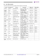
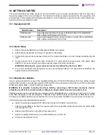
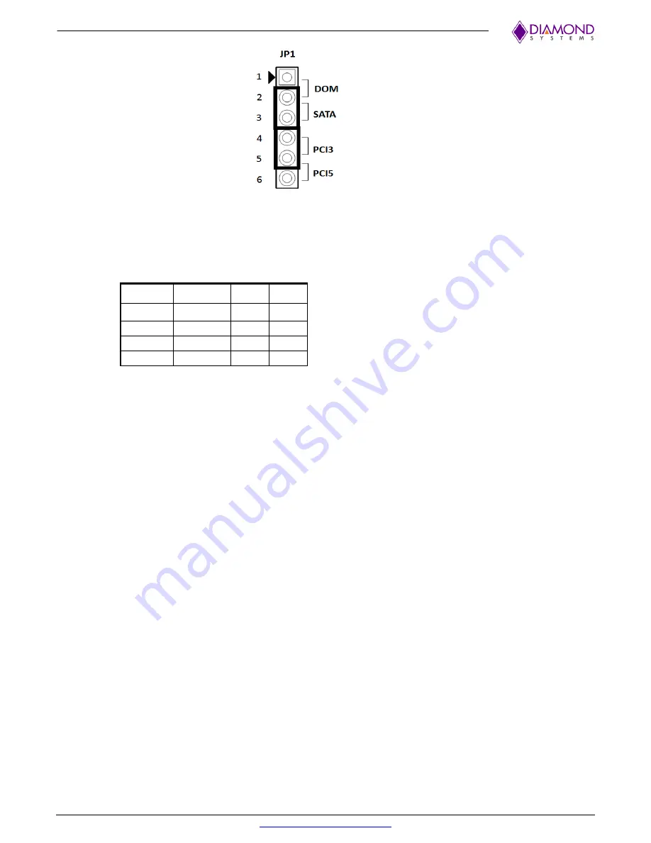
Figure 4 Jumper Block JP1 


The following table shows the different combinations of jumper block JP1. The row in bold and italics shows the 
default configuration of jumper block JP1. 


1-2 

2-3 

4-5 

5-6 

In 

Out 

In 

Out 

In 

Out 

Out 

In 

Out 

In 

In 

Out 

Out 

In 

Out 

In 

Note:    

1.  Jumpers should be installed in either positions 4-5 or 5-6. 


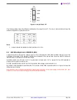
8.2  LVDS Backlight and LVDS VDD (JP2) 

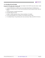
Jumper block JP2 configures the voltage supply for the LCD backlight, LVDS VDD and DIO Voltage as well. The 
orientation of the block in the diagrams matches the orientation of the jumper block when the board is rotated so 
that the Power in connector is on the lower edge. 

Available  options  are  +5V  and  +12V.  5V  is  generated  on  board  and  +12V  is  needed  for  the  LCD  backlight,  is 
powered via the power connector J12. 

For DIO, available options are 5V and 3.3V. By default, DIO voltage is provided with 3.3V 

By default, LVDS backlight is provided with +12V and the LVDS VDD is provided with 3.3V.  Figure 5 shows the 
default jumper locations. 

Note  that  the  +12V  is  directly  supplied  from  Input  power  connector.  If  the  Input  supply  is  other  than  12V,  user 
should not mount this jumper and supply the LCD backlight externally. 

Summary of Contents for Venus VNS563-4GD

Page 1: ...et Sunnyvale CA 94086 USA support diamondsystems com Tel 1 650 810 2500 Fax 1 650 810 2525 www diamondsystems com Revision Date Comment 1 00 03 13 2017 Initial Release 1 1a 06 20 2017 Power Supply and Thermal Solutions section updated 1 1b 08 24 2017 Updated JP2 jumper section 1 1c 08 31 2017 Updated Digital IO spec and connector mating parts 1 1d 09 11 2017 Updated default jumper settings and Vid...

Page 2: ...4 5 Board Layout Connector and Jumper Locations 15 6 I O Connectors 17 6 1 Connector Pin out and Signal Description 17 6 1 1 Power In J12 17 6 1 2 External Battery J14 17 6 1 3 USB 2 0 Ports J4 17 6 1 4 USB 3 0 Port J18 J19 19 6 1 5 Serial Ports J6 J7 19 6 1 6 Ethernet J16 19 6 1 7 SATA J3 20 6 1 8 SATA DOM J20 20 6 1 9 SATA DOM Power J21 20 6 1 10 Audio J8 20 6 1 11 LVDS LCD J11 21 6 1 12 LCD Bac...

Page 3: ... Installing OS and Booting 34 11 Video Features 35 12 Serial Ports and System Console 36 12 1 Configuration 36 12 2 Console redirection 36 13 Digital I O 37 14 Software driver overview 38 15 Thermal Solutions 39 15 1 Heat Spreader Drawing 39 15 2 Mounting Hole Specifications 39 15 3 Heat Spreader Installation 40 15 4 Heat Spreader Installed on the Board 41 15 5 Heat Spreader with brackets Installe...

Page 4: ... to avoid possible shorting from this type of damage However these design rules are not sufficient to prevent damage in all situations A third cause of failure is when a metal screwdriver tip slips or a screw drops onto the board while it is powered on causing a short between a power pin and a signal pin on a component This can cause overvoltage power supply problems described below To avoid this ...

Page 5: ...acceptable range of voltages connected to digital I O signals is 0 5V and they can withstand about 0 5V beyond that 0 5 to 5 5V before being damaged However logic signals at 12V and even 24V are common and if one of these is connected to a 5V logic chip the chip will be damaged and the damage could even extend past that chip to others in the circuit Bent connector pins This type of problem is ofte...

Page 6: ...600U 2 6GHz Turbo up to 3 4GHz 4MB Cache 15W TDP i5 6300U 2 4GHz Turbo up to 3 0GHz 3MB Cache 15W TDP Memory On board 4GB DDR4 Expandable over rugged SODIMM Up to 16GB Ethernet 1 10 100 1000 Mbps direct from processor 1 10 100 1000 Mbps using one PCIe x1 lane SATA 1 port direct from processor to standard SATA connector 1 port direct from processor to SATA DOM 1 port direct from processor to mSATA ...

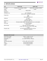
Page 7: ...m factor 146 x 102mm 5 75 x 4 00 Cooling Conduction cooling bottom side heat spreader Power input 9V to 18VDC in 12V Typical Operating Temp 40 C to 85 C at outer surface of heat spreader Shock Designed to meet MIL STD 202G Method 213 B Table 213 1 Condition A 50G 11ms half sine non operational Vibration Designed to meet MIL STD 202G Method 214A Table 214 1 Condition D 11 95G random vibration 15 mi...

Page 8: ...ATA Socket SATA PCIe One Bank 1x USB 2 0 SATA 7Pin VGA Chrontel CH7517 DDI2 PCI 104 Con SATA NXP CBTL2004 Transceiver SP336 Exar XR28V384 Transceiver SP336 LPC 2x UART 2 x USB2 0 2x USB 2 0 2 x USB3 0 2x USB 3 0 2x USB2 0 2 x USB3 0 2x USB 3 0 2x USB2 0 HDMI DDI1 Utility Con I2C1 LED DDR4 SODIMM 4GB 8GB 16GB DDR4 CH2 NXP PCA9535 I2C0 16 Bit PU PD Select PIC SATA DOM SATA Camera x2 2x MIPI CSI x1 I...

Page 9: ...cessary magnetics for both ports For increased ruggedness Ethernet connection is via a latching pin header not an RJ 45 jack The two magnetics components are placed back to back on the PCB to conserve PCB space On board LEDs are provided for Link Activity and Speed The LEDs are located along the board edge near the Ethernet connector The GbE ports use dual row 1 25mm pitch latching connectors The ...

Page 10: ... resistors for RS 422 485 are controlled using GPIO pins from the processor and are configurable via BIOS configuration screens as well as via application software Console redirection feature using a serial port for keyboard input and terminal display via a link to a second computer is provided in the BIOS on COM1 3 1 9 Digital IO The board provides 16 Digital I O signals with selectable 5V 3 3V l...

Page 11: ...CIe 104 including Type 1 Type 2 and OneBank Port 4 on the connector is left unconnected due to the limited supply of PCIe x1 lanes PCIe lane 1 on the connector is direct from the processor while lanes 2 and 3 come from a PCIe expansion switch 3 1 14 PCIe link routing Link 1 OneBank PCIe 104 connector Lane 1 Link 2 PCIe Minicard 1 Link 3 Processor GbE Link 4 I210 GbE Link 5 PCIe to PCI Bridge for P...

Page 12: ...fault settings can be saved without a battery Customizable splash screen Quiet boot option Enable disable for individual COM ports Protocol selection for each of the COM ports 120 ohm line termination control for serial ports in RS 422 485 protocol IRQ sharing for COM ports Enable disable Digital I O ports A and B Direction control Input Output for Digital I O ports A and B Wake on LAN for on boar...

Page 13: ...d options The figures below are the design limits of the board When converting the lower voltage current to main 12V input current an 85 efficiency factor should be used 12V 5V 3 3V Feature 1 0A 2 0A 2 0A PCI 104 and One Bank modules 3 0A PCIe Minicard add on modules 0 25A SATA disk module 1 4A 0 7A LCD power 1 1A LCD backlight 0 05A Utility connector 1 0A USB 2 0 ports 3 6A USB 3 0 port The 5V an...

Page 14: ...v 1 1d www diamondsystems com Page 14 4 MECHANICAL BOARD DRAWING Dimensions are in inches mm Connector dimensions indicate the center of the pad for pin 1 pin A1 for the PCI 104 connector Figure 2 Mechanical Board Drawing ...

Page 15: ...systems com Page 15 5 BOARD LAYOUT CONNECTOR AND JUMPER LOCATIONS JP2 LED Block 1 J20 J19 J18 J17 LED Block 7 LED Block 5 LED Block 6 J23 J16 J1 J15 J14 J13 J12 LED Block 2 LED Block 3 LED Block 4 J21 J11 J10 J22 J9 J2 J3 J4 JP1 J5 J6 J7 J8 ...

Page 16: ... Middle LED mPCIe 1 LAN J9 VGA Bottom LED mPCIe 1 PAN J10 HDMI LED Block 3 J11 LVDS LCD Top LED mPCIe 2 WAN J12 Power In Middle LED mPCIe 2 LAN J13 LVDS Backlight Bottom LED mPCIe 2 PAN J14 External Battery LED Block 4 J15 Digital IO Top LED BIOS LED J16 GbE Port 0 1 Middle LED Power On LED J17 MIPI Camera Bottom LED Power In LED J18 USB3 0 Port 1 3 LED Block 5 J19 USB3 0 Port 2 4 Top LED GBE0 ACT...

Page 17: ...mption is 6uA with RTC voltage at 3 0V while the system is in a mechanical off G3 state at room temperature This data can be used to estimate the battery life The voltage of the battery can affect the RTC accuracy In general when the battery voltage decays the RTC accuracy also decreases Example batteries are Duracell 2032 2025 or 2016 or equivalent which can give many years of operation Batteries...

Page 18: ...Venus User Manual Rev 1 1e www diamondsystems com Page 18 ...

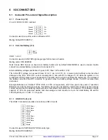
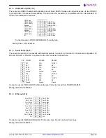
Page 19: ...re two serial port connectors with identical pinouts two ports per connector All ports are configurable for RS 232 RS 422 or RS 485 The pinout for the first connector is shown here Pin RS 232 RS 422 RS 485 1 TX1 TX1 TX RX 1 2 RX1 RX1 NC 3 RTS1 TX1 TX RX 1 4 CTS1 RX1 NC 5 Ground Ground Ground 6 TX2 TX2 TX RX 2 7 RX2 RX2 NC 8 RTS2 TX2 TX RX 2 9 CTS2 RX2 NC 10 Ground Ground Ground Connector used is S...

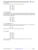
Page 20: ...ce and 5V is used for a board mounted SATA flash disk module The 5V is connected via a resettable fuse 1 Ground 2 SATA 1 TX 3 SATA 1 TX 4 Ground 5 SATA 1 RX 6 SATA 1 RX 7 Ground 5V 6 1 9 SATA DOM Power J21 If a SATA DOM module without pin 7 power is used then it will have a separate power connector to supply 5VDC Connector J21 may be used for this purpose DSC does not offer a cable 1 5V 2 Ground C...

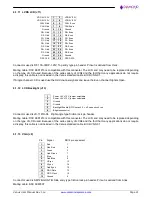
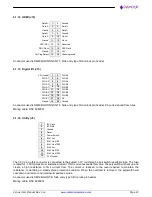
Page 21: ... kit CK VNS 01 If Single channel LCD is used use the Odd channel signals and leave the Even channel Signals Open 6 1 12 LCD Backlight J13 1 Power 5V 12V jumper selectable 2 Power 5V 12V jumper selectable 3 Ground 4 Ground 5 Backlight Enable GPIO output 0 off open circuit on 6 Brightness control Connector used is JS 1147H 06 Right angle type friction lock pin header Mating cable DSC 6981210 is comp...

Page 22: ...ck pin header Pinout is derived from Aries Mating cable DSC 6980501 6 1 16 Utility J5 1 I2C Clock 2 I2C Data 3 Ground 4 Reset 5 Power Switch 6 Eth 1 Act 7 Eth 1 Link 100 8 Eth 1 Link 1000 9 Eth 2 Act 10 Eth 2 Link 100 11 Eth 2 Link 1000 12 3 3V fused The 3 3V pin on this connector is connected to the system 3 3V rail through a polyswitch resettable fuse The fuse is rated for 100mA maximum sustaine...

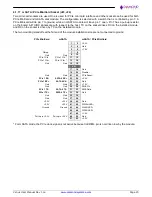
Page 23: ...the installed module The two mounting standoffs at the far end of the module installation site are not connected to ground PCIe MiniCard mSATA mSATA PCIe MiniCard 1 2 3 3V 3 4 Gnd 5 6 1 5V Clkreq 7 8 Gnd Gnd 9 10 PCIe 1 Clk PCIe 1 Clk 11 12 PCIe 1 Clk PCIe 1 Clk 13 14 Gnd Gnd 15 16 KEY 17 18 Gnd 19 20 Disable Gnd Gnd 21 22 PCIe Reset PCIe 1 RX SATA 0 RX 23 24 3 3V PCIe 1 RX SATA 0 RX 25 26 Gnd Gnd...

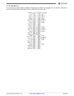
Page 24: ...PCIe Reset 3 3V 3 4 3 3V USB_1 5 6 USB_0 USB_1 7 8 USB_0 Ground 9 10 Ground PCIe1 Tx 11 12 PCIe0 Tx PCIe1 Tx 13 14 PCIe0 Tx Ground 15 16 Ground PCIe2 Tx 17 18 PCIe2 Tx 19 20 Ground 21 22 Ground PCIe1 Rx 23 24 PCIe0 Rx PCIe1 Rx 25 26 PCIe0 Rx Ground 27 28 Ground PCIe2 Rx 29 30 PCIe2 Rx 31 32 Ground 33 34 Ground PCIe1 Clk 35 36 PCIe0 Clk PCIe1 Clk 37 38 PCIe0 Clk 5VSB 39 40 5VSB PCIe2 Clk 41 42 PCIe...

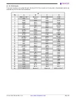
Page 25: ...D11 VI O AD10 M66EN 7 AD14 AD13 GND AD12 8 3 3V C BE1 AD15 3 3V 9 SERR GND SB0 PAR 10 GND PERR 3 3V SDONE 11 STOP 3 3V LOCK GND 12 3 3V TRDY GND DEVSEL 13 FRAME GND IRDY 3 3V 14 GND AD16 3 3V C BE2 15 AD18 3 3V AD17 GND 16 AD21 AD20 GND AD19 17 3 3V AD23 AD22 3 3V 18 IDSEL0 GND IDSEL1 IDSEL2 19 AD24 C BE3 VI O IDSEL3 20 GND AD26 AD25 GND 21 AD29 5V AD28 AD27 22 5V AD30 GND AD31 23 REQ0 GND REQ1 VI...

Page 26: ...cal Generic 6989101 SATA DOM Power Hirose DF13C 2P 1 25V 2 pos 1 25mm pitch vertical latching DF13 2S 1 25C 6980511 Audio JST SM08B GHS TB 8 pos 1 25mm pitch Right angle latching GHR 08V S 6980508 LCD Hirose DF13A 30DP 1 25V 40 pos 050 pitch dual row vertical latching DF13 30DS 1 25C LCD backlight Chyao Shiunn JS 1147H 06 6 pos 1 25mm pitch Right angle JS 1146 06 VGA JST SM12B GHS TB 12 pos 1 25mm...

Page 27: ...Utility J5 2 6980517 Digital I O J15 3 6980507 VGA J9 4 6980508 Audio J8 5 6989101 SATA J20 J3 6 6980513 Ethernet J16 7 6980500 Serial ports J6 J7 8 6980100 USB 3 0 J18 J19 9 6980503 USB 2 0 J4 10 6980524 Battery J14 11 6980512 Power in J12 12 6980519 HDMI J10 Note HDMI cable only available in CK VNS 02 cable kit Figure 2 I O Cables ...

Page 28: ... Default Jumper locations Jumper Description JP1 SATA DOM Power PCI VIO JP2 LVDS LCD VCC and Backlight 8 1 SATA DOM Power PCI VIO JP1 The 7th pin of the SATA connector J20 can be configured for SATA DOM or for SATA cable By default 7th pin of J20 is connected to ground for the SATA cable The IO voltage of PCI data address lines can be configured for 3 3V or 5V The default jumper location is shown ...

Page 29: ...as well The orientation of the block in the diagrams matches the orientation of the jumper block when the board is rotated so that the Power in connector is on the lower edge Available options are 5V and 12V 5V is generated on board and 12V is needed for the LCD backlight is powered via the power connector J12 For DIO available options are 5V and 3 3V By default DIO voltage is provided with 3 3V B...

Page 30: ...f jumper locations on JP2 1 2 2 3 4 5 5 6 LVDS Backlight LVDS VDD In Out In Out 12V 5V In Out Out In 12V 3 3V Out In In Out 5V 5V Out In Out In 5V 3 3V 7 8 8 9 DIO Voltage In Out 3 3V Out In 5V Note 1 Voltage supply on LVDS backlight will not depend on or affect the voltage input of LVDS 2 Do not install a jumper on 3 4 6 7 positions ...

Page 31: ...ugh SHELL Utility 5 In BOOT menu enter launch shell based file systems to boot to shell Make sure that Shell based USB flash disk is connected to one of the USB ports 6 Once booted to shell identify which is the file system for USB flash disk It can be fs0 or fs1 or fs2 You can check this by pressing page up button 7 Make sure that afuefix64 efi utility and BIOS file that need to programmed are av...

Page 32: ...lank screen or custom splash screen if available Quick boot turns off memory test during startup to save time To enable these features go to the Boot menu then select Boot Settings Configuration Diamond can provide custom splash screens upon request from an image file 9 8 Serial Port Configuration Venus SBC supports 4 serial ports All the 4 ports support RS 232 422 485 functionalities The function...

Page 33: ...rrectly will destroy the Venus SBC 5 For a quick verification that the system is set up and working properly if no boot device is attached the system will boot to BIOS mode 10 3 Boot Device Options Venus can boot from SATA or any of the available USB ports or PXE 10 100 Ethernet Port only Either a board powered SATA DOM or an externally powered SATA HDD can be connected to the SATA port DSC will p...

Page 34: ...d having Windows 10 installation image Boot the Venus board to BIOS The SATA HDD and USB device should be detected in BIOS under boot devices Under boot priorities set highest priority for USB Save BIOS settings and restart Windows 10 installer would start running Follow the instructions in the installer Upon successful installation boot to Windows 10 and install the necessary drivers For installi...

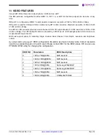
Page 35: ...1920 x 1080 x 60Hz x 24bpp The LCD backlight control is provided by a PWM circuit LCD backlight power and control are on a separate latching connector BIOS will support option for selecting Single channel Dual Channel Color Depth resolution and brightness control By default BIOS will support 7 EDID configuration Emulation as shown in below table Correct resolution need to be selected based on the ...

Page 36: ...422 485 modes The modes can be configured in BIOS Both TX and RX termination selection option are available under BIOS menu 12 2 Console redirection Connect any of the Venus serial ports to PC In BIOS menu go to Advanced settings menu then in Remote Access Configuration enable the Remote access feature Then select the serial port User should see the BIOS setup menu in the PC console ...

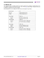
Page 37: ... resistors Each 8bit digital IOs can be configured for PU PD Below are the digital IO specification No of IO lines 16 Direction Programmable bit by bit Polarity Programmable bit by bit Input voltage VDD 5V Logic 0 0 0V min 1 5V max 1uA Logic 1 3 5V min 5 5V max 1uA Output Voltage VDD 5V Logic 0 0 0V min 0 7V max 14mA Typ Logic 1 4 1V min 5 0V max 10mA Typ Input voltage VDD 3 3V Logic 0 0 0V min 0 ...

Page 38: ...M installed with either Windows 10 or Linux All the necessary I O drivers are also available as part of the Development Kit Please contact Diamond Systems for more details Some of the drivers that are required with the Windows 10 operating system are given below These drivers are available for download from Diamond Systems website 1 Audio Driver 2 Chipset Driver 3 Gigabit Ethernet Driver 4 Graphic...

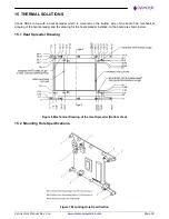
Page 39: ... is mounted on the bottom side of the board The mechanical drawing of the heat spreader and the drawing for the heat spreader installed on the board are shown below 15 1 Heat Spreader Drawing Figure 6 Mechanical Drawing of the Heat Spreader Bottom View 15 2 Mounting Hole Specifications Figure 7 Mounting Hole Specification ...

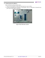
Page 40: ...e ESD safe handling procedures always 1 Inspect the Heat Spreader and make sure thermal pads are in good condition 2 Remove all thermal pad liners from bottom of heat spreader Avoid any contamination of exposed thermal pad surfaces Refer Figure 8 for reference Figure 8 Thermal Pad liners location ...

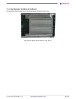
Page 41: ... Manual Rev 1 1e www diamondsystems com Page 41 15 4 Heat Spreader Installed on the Board Figure below shows the side view of the heat spreader installed on the Board Figure 9 Heat Spreader Installed on the board ...

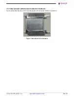
Page 42: ... 1 1e www diamondsystems com Page 42 15 5 Heat Spreader with brackets Installed on the Board Figure below shows the side view of the heat spreader with the bracket installed on the Board Figure 10 Heat Spreader with Bracket ...

Page 43: ...B2 0 Serial ports 4 RS 232 422 485 ports Audio HD Audio ALC892 CODEC with stereo line out line in and microphone Networking Two 10 100 1000Mbps Ethernet ports Mass storage 1 SATA port for external hard drive 1 SATA port for external hard drive or SATA DOM 1 mSATA Expansion bus PC 104 PCI Bus One Bank PCIe connector 2 Mini PCIe Full card size System input voltage 9VDC to 18VDC Typ 12V Power consump...

Reviews: