background image

www.d

fi

 .com

Chapter 2 Hardware Installation

24

Chapter 2

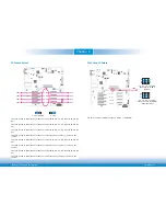
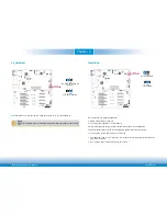
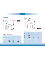
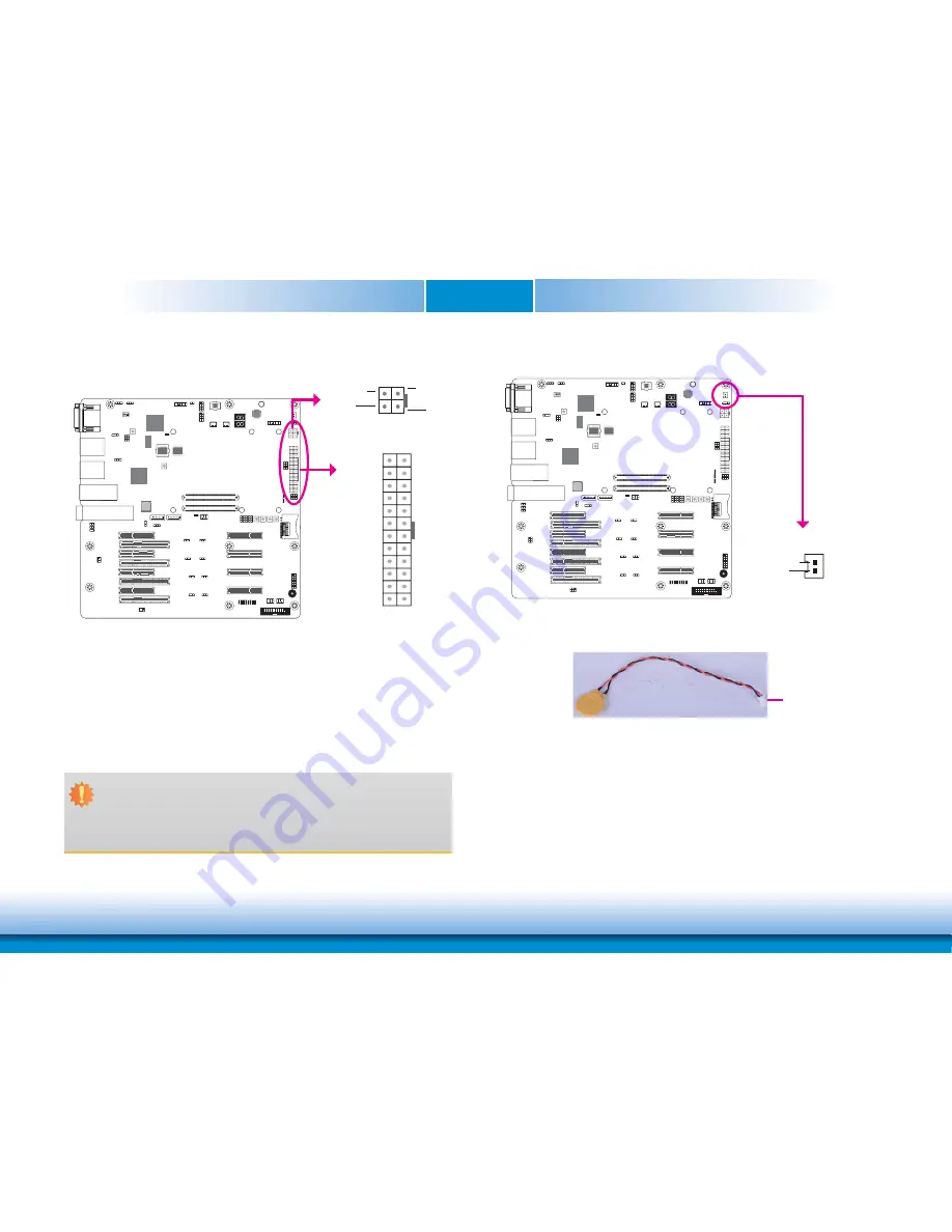
Use a power supply that complies with the ATX12V Power Supply Design Guide Version 1.1. 

An ATX12V power supply unit has a standard 24-pin ATX main power connector that must be 

inserted into the 24-pin connector. The 4-pin +12V power connector enables the delivery of 

more +12VDC current to the COM express module board and carrier board’s PCIe device. 

The power connectors from the power supply unit are designed to fit the 24-pin and 4-pin 

connectors in only one orientation. Make sure to find the proper orientation before plugging 

the connectors.

Power Connectors

1

ON

2 3 4

1 3

2 4

Ground

Ground

+12V

+12V

Important:

The system board consumes a minimal amount of power. Due to its low power 

consumption, you only need a 120W to 150W power supply. Every power supply has 

its minimum load of power. If you use a greater than 150W power supply, the power 

consumed by the system board may not attain its minimum load causing instability to 

the entire system.

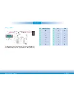
13

12 24

1

+3.3VDC

+3.3VDC

+5VDC

PWR_OK

+5VSB

+12VDC

+12VDC

+3.3VDC

+3.3VDC

-12VDC

PS_ON#

GND

GND

NC

+5VDC

+5VDC

+5VDC

GND

GND

GND

GND

GND

+5VDC

GND

1

ON

2 3 4

Battery

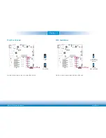
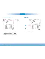
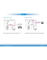
The lithium ion battery (CR2032 coin cell) powers the real-time clock and CMOS memory. It is 

an auxiliary source of power when the main power is shut off.

Safety Measures

• Danger of explosion if battery incorrectly replaced.

• Replace only with the same or equivalent type recommended by the manufacturer.

• Dispose of used batteries according to local ordinance

.

Connect to the 

battery connector

Battery

Battery 

Connector

1

+3.3V

GND

2

Summary of Contents for COM333-I

Page 1: ...www dfi com Chapter 1 Introduction 1 COM333 I COM Express Carrier Board User s Manual A47100832 Preliminary Version ...

Page 2: ... owners FCC and DOC Statement on Class B This equipment has been tested and found to comply with the limits for a Class B digital device pursuant to Part 15 of the FCC rules These limits are designed to provide reason able protection against harmful interference when the equipment is operated in a residential installation This equipment generates uses and can radiate radio frequency energy and if ...

Page 3: ... Location Select 12 PIN 0 3 DIO Output Input Select 12 VCC5_IN Power Select 13 ATX AT Mode Select Power_OK 13 PS_ON Select 14 Clear CMOS 14 BMC UART1 Port Mode Select 15 BMC UART1 Driver s Receiver s Power Rail Select 15 BMC SPI1 Interface Mode Select 16 BMC 2nd Boot Watchdog Timer Select 16 BMC MAC 1 Interface Type Select 17 BMC VGA Select 17 Rear Panel I O Ports 18 Graphics Interface 18 COM Seri...

Page 4: ...ent electrostatic build up leave the system board in its anti static bag until you are ready to install it 2 Wear an antistatic wrist strap 3 Do all preparation work on a static free surface 4 Hold the device only by its edges Be careful not to touch any of the components contacts or connections 5 Avoid touching the pins or contacts on all modules and connectors Hold modules or con nectors by thei...

Page 5: ...the package may not come similar to the information listed above This may differ in accordance with the sales region or models in which it was sold For more information about the standard package in your region please contact your dealer or sales representative Before Using the System Board Before using the system board prepare basic system components If you are installing the system board in a ne...

Page 6: ... remote management USB 4 x USB 3 0 2 0 Serial 1 x RS 232 DB 9 supports by BMC which default is debug port and may switch to normal RS 232 INTERNAL I O Serial 2 x Serial Interface Connectors TX RX 2 0mm pitch SATA 2 x SATA 3 0 up to 6Gb s DIO 1 x 8 bit DIO 4 input 4 output 1 x SDIO available upon request LPC 1 x LPC SMBus 1 x SMBus BMC Features 1 IPMI 2 0 2 Web Browser Support 3 Web Interface 4 iKV...

Page 7: ... JP29 ATX AT Mode Select Power_OK JP27 PS_ON Select JP28 Front Panel System Fan2 1 1 System Fan1 1 1 1 B110 A110 B1 A1 COM Express Connector D110 C110 D1 C1 COM Express Connector 1G MGMT LAN USB 2 3 USB 3 0 10G RJ 45 LAN 3 4 1 1 1 5 1 6 2 1 1 2 1 5 I 2 C HDR Battery 1 PIN GPO0 3 DIO Output JP24 PIN GPI0 3 DIO Input JP25 10G PHY CAP 2 3 Select JP9 1 SATA 0 BMC UART1 Driver s Receiver s Power Rail S...

Page 8: ... 0 Ports 2 3 JP2 2 3 On 5VDU 1 2 On 5V default 3 1 2 3 1 2 Important If your module board supports Wake On USB Keyboard Mouse function the 5V_ standby power source of your power supply must support 2A for 2 USB devices Function Test Jumper Battery Low Indicator 1 ON 2 3 4 J4 This jumper is used to simulate the signal status that indicates the external battery is low By setting J4 pins 1 and 2 to O...

Page 9: ...nterfaces 0 and 1 can be configured by either I2 C or by MDIO If the Carrier leaves the line NC then this indicates to the Module that the Carrier PHY can only be configured by MDIO 1 3 2 1 3 2 JP19 2 3 On MDIO or I2 C 1 2 On MDIO only default 3 1 2 3 1 2 1 2 On MDIO only default 2 3 On MDIO or I2 C 1 ON 2 3 4 USB 2 0 Port 3 Select The JP4 is used to select the USB 2 0 port 3 connection path JP4 1...

Page 10: ...or PCIe2 x8 slot 2 3 On The JP12 is used to select the PCIe Lanes 16 19 PCIe7 x4 slot 1 2 On or PCIe3 x8 slot 2 3 On The JP16 is used to select the PCIe Lanes 20 23 PCIe11 x4 slot 1 2 On or PCIe3 x8 slot 2 3 On The JP13 is used to select the PCIe Lanes 24 27 PCIe8 x4 slot 1 2 On or PCIe4 x8 slot 2 3 On The JP17 is used to select the PCIe Lanes 28 31 PCIe12 x4 slot 1 2 On or PCIe4 x8 slot 2 3 On JP...

Page 11: ...on CB Select The JP20 is used to select to turn on or off the TPM_PP on CB 1 3 2 1 3 2 JP20 1 2 On On 2 3 On Off default 1 ON 2 3 4 ESPI Enable Select The JP21 is used to select to enable LPC BUS or ESPI BUS 1 3 2 1 3 2 JP21 1 2 On LPC BUS Enable default 2 3 On ESPI BUS Enable ...

Page 12: ...2 1 3 2 JP22 2 3 On JP23 2 3 On SPI0 on Module default 1 3 2 1 3 2 JP22 2 3 On JP23 1 2 On SPI0 on Carrier 1 3 2 JP22 1 2 On JP23 1 2 On Module SPI Only 1 ON 2 3 4 PIN 0 3 DIO Output Input Select The JP24 and JP25 are used to select PIN 0 3 DIO output and input respectively 3 1 2 JP24 1 2 4 5 7 8 10 11 On LED off 3 1 2 12 10 11 12 10 11 JP25 2 3 5 6 8 9 11 12 On LED on default ...

Page 13: ...lt 3 4 On 5V 5 6 On NC 5 1 3 2 4 6 5 2 4 6 1 3 5 2 4 6 1 3 ATX AT Mode Select Power_OK 1 ON 2 3 4 JP27 The JP27 allows you to select the PWR_OK connection state when setting power at ATX or AT mode 1 3 2 1 3 2 1 2 On PWR_OK from ATX PS PWR_OK default 2 3 On PWR_OK from BMC GPO 1 3 2 1 X No PWR_OK when in AT Mode Note JP27 and JP28 need to be set simultaneously Please refer next page for JP28 descr...

Page 14: ...ower off the system and unplug the power cord 2 Set JP29 pins 2 and 3 to On Wait for a few seconds and set JP29 back to its default set ting pins 1 and 2 On 3 Now plug the power cord and power on the system 1 2 On Normal default 2 3 On Clear CMOS 1 ON 2 3 4 JP29 3 1 2 3 1 2 PS_ON Select 1 ON 2 3 4 JP28 The JP28 allows you to select the ATX mode auto power on or AT mode always on 1 3 2 1 3 2 1 2 On...

Page 15: ... 2 3 4 JP31 3 1 2 3 1 2 BMC UART1 Port Mode Select 1 ON 2 3 4 JP30 The JP30 is used to select the mode of BMC UART1 port 1 3 2 1 3 2 1 2 On Normal UART 2 3 On Debug mode default The JP31 is used to select the driver s receiver s power rail of the BMC UART1 Note JP30 and JP31 need to be set simultaneously Note JP30 and JP31 need to be set simultaneously ...

Page 16: ...1 BMC SPI1 Interface Mode Select SW1 Pins 1 2 Disable SPI Interface default 1 Off 2 Off Enable SPI Master 1 Off 2 On Reserved 1 On 2 Off Enable SPI Pass Through 1 On 2 On BMC 2nd Boot Watchdog Timer Select 1 ON 2 3 4 SW1 To enable or disable BMC 2nd boot watchdog timer please use pin 3 of finger switch SW1 BMC 2nd Boot Watchdog Timer Select SW1 Pin 3 Disable Off Enable default On ...

Page 17: ...N 2 3 4 SW1 To select BMC MAC 1 interface type please use pin 4 of finger switch SW1 BMC MAC 1 Interface Type Select SW1 Pin 4 RMII NCSI Off RGMII default On BMC VGA Select 1 ON 2 3 4 J20 1 2 1 2 1 X On Normal VGA 2D default 1 2 On Disable VGA This jumper is used to disable BMC integrated VGA ...

Page 18: ...P LAN ports BMC UART1 Debug 10G SFP LAN 1 2 USB 3 0 2 3 1G MGMT LAN 1G RJ 45 LAN 1 VGA USB 3 0 0 1 10G RJ 45 LAN 3 4 Graphics Interface The display port consists of the following 1 VGA port 1 ON 2 3 4 VGA The VGA port is used for connecting a VGA monitor Connect the monitor s 15 pin D shell cable connector to the VGA port After you plug the monitor s cable connector into the VGA port gently tighte...

Page 19: ...ible UARTs that can be used with modems serial printers remote display terminals and other serial devices 1 ON 2 3 4 BMC UART1 RS232 BMC UART1 Debug 2 1 9 COM 1 COM 2 Pin COM1 COM2 1 NC NC 2 RX1 RX2 3 TX1 TX2 4 NC NC 5 GND GND 6 NC NC 7 NC NC 8 NC NC 9 NC NC 1 2 3 4 5 6 7 8 9 Pin BMC UART 1 Debug 1 DCD 2 RD 3 TD 4 DTR 5 GND 6 DSR 7 RTS 8 CTS 9 RI ...

Page 20: ...orts 0 1 and JP2 for USB 3 0 ports 2 3 must be set to 2 3 On 5VDU Refer to USB Power Select in this chapter for more information Important If your module board supports Wake On USB Keyboard Mouse function the 5V_ standby power source of your power supply must support 2A for 2 USB devices USB Ports USB allows data exchange between your computer and a wide range of simultaneously acces sible externa...

Page 21: ...ned by Intel Corporation to facilitate the industry s transition towards legacy free systems It allows the integration of low bandwidth legacy I O components within the system which are typically provided by a Super I O controller Further more it can be used to interface firmware hubs Trusted Platform Module TPM devices and embedded controller solutions Data transfer on the LPC bus is implemented ...

Page 22: ...nect Serial ATA devices Connect one end of the Se rial ATA cable to a SATA connector and the other end to your Serial ATA device Cooling Fan Connectors The fan connectors are used to connect cooling fans The cooling fans will provide adequate airflow throughout the chassis to prevent overheating the CPU and system board components 1 ON 2 3 4 1 3 Sense Power Ground System Fan 2 System Fan 1 ...

Page 23: ...a multi master bus I2 C Header 1 ON 2 3 4 I2 C SMBus Header The SMBus System Management Bus connector is used to connect the SMBus device It is a multiple device bus that allows multiple chips to connect to the same bus and enable each one to act as a master by initiating data transfer 1 ON 2 3 4 2 GND 3 3V DU SMBUS_Data SMBUS_CLK SMBUS_Alert 1 5 2 1 NC I2 C_DATA I2 C_Clock GND 3V3 DU 5 SMBus ...

Page 24: ...sumes a minimal amount of power Due to its low power consumption you only need a 120W to 150W power supply Every power supply has its minimum load of power If you use a greater than 150W power supply the power consumed by the system board may not attain its minimum load causing instability to the entire system 13 12 24 1 3 3VDC 3 3VDC 5VDC PWR_OK 5VSB 12VDC 12VDC 3 3VDC 3 3VDC 12VDC PS_ON GND GND ...

Page 25: ...hen the hard drive is being accessed RESET Reset Switch This switch allows you to reboot without having to power off the system PWR LED Power Standby LED When the system s power is on this LED will light When the system is in the S1 POS Power On Suspend state it will blink every second When the system is in the S3 STR Suspend To RAM state it will blink every 4 seconds ATX SW ATX Power Switch This ...

Page 26: ...her cards that comply to the PCI Express specifications into the PCI Express x8 slot 1 ON 2 3 4 PCIe 5 PCIe x4 PCIe 1 PCIe x8 PCIe 6 PCIe x4 PCIe 2 PCIe x8 PCIe 7 PCIe x4 PCIe 3 PCIe x8 PCIe 8 PCIe x4 PCIe 4 PCIe x8 PCIe 9 PCIe x4 PCIe 10 PCIe x4 PCIe 11 PCIe x4 PCIe 12 PCIe x4 COM Express Connectors The COM Express connectors are used to interface the carrier board with a COM Express board Refer ...

Page 27: ...D 38 10G_SFP_SDA1 10G_SFP_SCL1 39 10G_SFP_SDA0 10G_SFP_SCL0 40 10G_SDP0 10G_SDP1 41 GND FIXED GND FIXED 42 10G_KR_RX1 10G_KR_TX1 43 10G_KR_RX1 10G_KR_TX1 44 GND GND 45 10G_PHY_MDC_SCL1 10G_PHY_MDIO_SDA1 USB0 USB1 USB2 USB3 USB2 USB3 USB_2_3_OC USB_0_1_OC PCIE_TX12 PCIE_RX12 PCIE_TX12 PCIE_RX12 GND FIXED GND FIXED PCIE_TX13 PCIE_RX13 PCIE_TX13 PCIE_RX13 GND GND RSVD I2C_CK BIOS_DIS0 ESPI_SAFS I2C_D...

Page 28: ...1 70 GND FIXED GND FIXED GND FIXED 71 PCIE_RX8 PCIE_RX22 PCIE_TX22 72 PCIE_RX8 PCIE_RX22 PCIE_TX22 73 GND GND GND 74 PCIE_RX9 PCIE_RX23 PCIE_TX23 75 PCIE_RX9 PCIE_RX23 PCIE_TX23 76 GND GND GND 77 PCIE_RX10 RSVD RSVD 78 PCIE_RX10 PCIE_RX24 PCIE_TX24 79 GND PCIE_RX24 PCIE_TX24 80 GND FIXED GND FIXED GND FIXED 81 PCIE_RX11 PCIE_RX25 PCIE_TX25 82 PCIE_RX11 PCIE_RX25 PCIE_TX25 83 GND RSVD RSVD 84 VCC_5...

Page 29: ...30 100 GND FIXED GND FIXED GND FIXED 101 FAN_PWMOUT PCIE_RX31 PCIE_TX31 SPI_POWER SPI_MISO GPO0 SD_CLK opt SPI_CLK GND FIXED SER1_TX SPI_MOSI TPM_PP TYPE10 SER0_TX SER0_RX 102 FAN_TACHIN PCIE_RX31 PCIE_TX31 103 SLEEP GND GND 104 VCC_12V VCC_12V VCC_12V 105 VCC_12V VCC_12V VCC_12V 106 VCC_12V VCC_12V VCC_12V 107 VCC_12V VCC_12V VCC_12V 108 VCC_12V VCC_12V VCC_12V 109 VCC_12V VCC_12V VCC_12V 110 GND...

Page 30: ...leep Note The Sleep and Lid functions are supported only when your operating system supports ACPI SDIO optional This expansion port is used to insert a Secure Digital Input Output SDIO or Multimedia Card MMC device Aside from storing data files an SDIO card is also capable of storing powerful software applications 1 ON 2 3 4 SDIO optional BMC AST2500 Chip Level Reset BMC AST2500 SOC Level Reset ...

Page 31: ...ator LED for Type 7 Module Inserted Indicator LED for Type 6 Module Inserted Debug LED GPI3 LED GPI2 LED GPI1 LED GPO0 LED GPO1 LED GPO2 LED GPO3 LED GPI0 LED Inphi Configure Pin Plug 1 ON 2 3 4 JP8 3 1 GND CS4227 SCL 1 8V CS4227 SDA 1 8V 0Hz Always dark means firmware is not running or dead 0 1Hz Abnormal mode some interrupts are not serviced for over 2 seconds 0 5Hz Normal operation mode ARM run...

Page 32: ...www dfi com Chapter 2 Hardware Installation 32 Chapter 2 eSPI Female Header 1 ON 2 3 4 eSPI Female Header The eSPI female header is reserved for future EXT module 2 1 14 13 ...

Reviews: