background image

40

DN-V750/V755

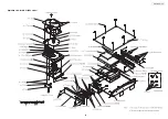
EXPLODED VIEW (for DN-V750 model)

Accessory

1

3

4

5

7

8

9

10

11

12

13

14

15

16

17

18

20

19

51

52

52

50

40

41

42

43

44

53

55

56

21

54

2

6

Parts  List

Parts marked with this symbol

have critical

characteristics.
Use ONLY replacement parts recommended by
the manufacturer.

WARNING:

 印の部分は安全を維持するために重要

な部品です。従って交換時は必ず指定の

部品を使用してください。

★ mark is the screw of


50

Summary of Contents for Professional DN-V755

Page 1: ...g instructions without fail For purposes of improvement specifications and design are subject to change without notice 本文中に使用しているイラストは 説明の都合上現物 と多少異なる場合があります 修理の際は 必ず取扱説明書を参照の上 作業を行っ てください サービスをおこなう前に このサービスマニュアルを 必ずお読みください 本機は 火災 感電 けがなど に対する安全性を確保するために さまざまな配慮を おこなっており また法的には 電気用品安全法 に もとづき 所定の許可を得て製造されております 従ってサービスをおこなう際は これらの安全性が維 持されるよう このサービスマニュアルに記載されて いる注意事項を必ずお守りください 本機の仕様は性能改良のため 予告なく変更す...

Page 2: ...nit to the customer make sure you make either 1 a leakage current check or 2 a line to chassis resistance check If the leakage current exceeds 0 5 milliamps or if the resistance from chassis to either side of the power cord is less than 460 kohms the unit is defective LASER RADIATION Do not stare into beam or view directly with optical instruments class 3A laser product 1 2 500V 1M 1 2 ...

Page 3: ...3 DN V750 V755 BLOCK DIAGRAM ...

Page 4: ...ay appear at the upper right of a monitor 3 Set VIDEO AUDIO PICTURE SCRIPT to VIDEO 6 Display Color bar 1 Press the STOP button pressing the SELECT button 2 Until the display appear at the upper right of a monitor 3 Press the STOP button to 1 pressing the SELECT button 4 Press the PLAY button and quickly press the PAUSE button Display Color bar with a still picture 7 Adjusting the output of Compos...

Page 5: ...OFF the 1 and 2 Dip switch on the back panel 4 Turn the power switch ON 5 VIDEO mode 1 Press the SELECT button about for 2 second 2 Until the display appear at the upper right of a monitor 3 Set VIDEO AUDIO PICTURE SCRIPT to VIDEO 6 Display Color bar 1 Press the STOP button pressing the SELECT button 2 Until the display appear at the upper right of a monitor 3 Press the STOP button to 1 pressing t...

Page 6: ...6 DN V750 V755 SEMICONDUCTORS Only major semiconductors are shown general semiconductors etc are omitted to list 主な半導体を記載しています 汎用の半導体は記載を省略しています 1 IC s EM8551B IC105 ...

Page 7: ...VID_D 18 O Not used 34 B7 VID_D 13 Video Output C 5 O Not used 35 B8 VID_D 9 Video Output C 1 O Not used 36 B9 VID_CLKIN Video Output Video Clock In 37 B10 VID_D 3 Video Output Y 3 O Not used 38 B11 VID_DVLD Video Output Video active Video valid O Not used 39 B12 PIO1 1 Programmable I O Port 1 Bit 1 I Lev Pu H L H L L Active 40 B13 PIO1 5 Programmable I O Port 1 Bit 5 O Pd L L H Active 41 B14 PIO1...

Page 8: ...used 100 D19 UART0_CTS UART0 Clear to Send I intPd Not used 101 D20 PIO0 2 Programmable I O Port 0 Bit 2 I Lev Pu H L H L L OSD Off H OSD On 102 D21 PIO0 4 Programmable I O Port 0 Bit 4 I Lev Pu H L H L L Active 103 D22 AVSS_SPLL System PLL Ground Connect to GND_D 104 D23 AVDD_SPLL System PLL Power Connect to 1 8V_A for System PLL 105 D24 AVDD_VPLL Video PLL Power Connect to 1 8V_A for System PLL ...

Page 9: ...D 166 H5 VSS_IO Connect to GND_D 167 H6 VSS_IO Connect to GND_D 168 H23 VSS_IO Connect to GND_D 169 H24 NC Not used 170 H25 SM_D 15 System Memory Data Bit15 I O Connect to system sdram D15 and flash chip D15 171 H26 SM_A 9 System Memory Address Bit9 O Connect to system sdram A9 and flash chip A9 172 H27 SM_A 8 System Memory Address Bit8 O Connect to system sdram A8 and flash chip A8 173 J1 DAC3_AC...

Page 10: ...M A1 231 N5 VDD_IO Connect to 3 3V_D 232 N11 VSS_IO Connect to GND_D 233 N12 VSS_IO Connect to GND_D 234 N13 VSS_IO Connect to GND_D 235 N14 VSS_IO Connect to GND_D 236 N15 VSS_IO Connect to GND_D 237 N16 VSS_IO Connect to GND_D 238 N17 VSS_IO Connect to GND_D 239 N23 VDD_CORE Connect to 1 8V_D for core 240 N24 SM_CLKE System Memory SDRAM Clock Enable O Connect to system sdram CLKE 241 N25 SM_D 18...

Page 11: ...ND_D 305 U16 VSS_IO Connect to GND_D 306 U17 VSS_IO Connect to GND_D 307 U23 VSS_IO Connect to GND_D 308 U24 SM_D 23 System Memory Data Bit23 I O Connect to system sdram D23 309 U25 SM_D 27 System Memory Data Bit27 I O Connect to system sdram D27 310 U26 SM_A 12 System Memory Address Bit12 O Connect to system sdram BA0 and flash chip A12 311 U27 SM_D 24 System Memory Data Bit24 I O Connect to syst...

Page 12: ... Data Bit 0 I O Connect to MPEG SDRAM D0 368 AC2 MM_D 15 Mpeg Memory Data Bit 15 I O Connect to MPEG SDRAM D15 369 AC3 MM_D 26 Mpeg Memory Data Bit 26 I O Connect to MPEG SDRAM D26 370 AC4 VIDIN_D 14 Video Input Data Bit 14 I intPd Not used 371 AC5 VSS_CORE Connect to GND_D 372 AC6 VDD_IO Connect to 3 3V_D 373 AC7 VDD_IO Connect to 3 3V_D 374 AC8 VSS_CORE Connect to GND_D 375 AC9 VDD_CORE Connect ...

Page 13: ...N V1500X 433 AE13 LPB_AD 2 Local Peripheral Bus Address Data bit 2 I O Connect to Ethernet DM9000 and CX303 for DN V1500X 434 AE14 DTACK RDY Local Peripheral Bus Transfer Acknowredge I Ed Pu H H ACK RDY WAIT signal input for local peripheral bus 435 AE15 LPB_WR Local Peripheral Bus Write Command O Connect to Ethernet DM9000 and CX241 for DN V1500X 436 AE16 DMA_REQ1 No Connection I intPd Connect to...

Page 14: ...ntPd Connect to CX303 for DN V1500X 480 AG6 VIDIN_HSYNC Video Input Hsync In I intPd Connect to CX303 for DN V1500X 481 AG7 NC No Connection Not used 482 AG8 NC No Connection Not used 483 AG9 NC No Connection Not used 484 AG10 LPB_AD 12 Local Peripheral Bus Address Data bit 12 I O Connect to Ethernet DM9000 and CX303 for DN V1500X 485 AG11 LPB_AD 8 Local Peripheral Bus Address Data bit 8 I O Conne...

Page 15: ... DGND NC LINK_O WAKEUP PW_RST DGND SD12 IOR 77 78 79 80 81 82 83 84 85 SD15 SD14 SD13 SD8 SD11 SD10 SD9 SA4 DVDD IO16 CMD SA8 SA5 SA6 SA7 SA9 DGND INT IOW AEN IOWAIT DVDD SD0 SD1 SD2 SD3 SD4 SD5 SD6 SD7 RST DGND TEST1 TEST2 TEST3 TEST4 DVDD X2_25M X1_25M DGND SD AGND AVDD AVDD RX RX AGND AGND TXO TXO AVDD DVDD LINK_I RXD0 RXD1 RXD2 RXD3 DGND CRS COL RX_DV RX_ER RX_CLK TEST5 TX_CLK TXD0 TXD2 TXD3 T...

Page 16: ...he polarity of the INT pin When the MDC pin is pull high the INT pin low active otherwise the INT pin is high active Processor interface 1 IOR I Processor Read command This pin is low active at default its polarity can be modified by EEPROM setting See the EEPROM content description for detail 2 IOW I Processor Write command This pin is low active at default its polarity can be modified by EEPROM ...

Page 17: ...n EEDO is pull high and WAKEUP is not pull high 57 IO32 in double word mode O Double word command indication This pins is used as the Double word command indication when the DM9000 is set to double data word mode and when the access of internal memory is double word width this pin will be asserted This pin is low active at default its polarity can be modified by EEPROM setting See the EEPROM conte...

Page 18: ...ernal PHY In LED mode 0 it is the LED of the carrier sense signal of the internal PHY only 10 100 PHY Fiber 24 SD I Fiber optic signal detect PECL signal which indicates whether or not the fiber optic receives pair is receiving valid levels 25 AGND Bandgap ground 26 BGRES I O Bandgap pin 27 AVDD Bandgap and guard ring power 28 AVDD RX power 29 RX I TP RX input 30 RX I TP RX input 31 AGND RX ground...

Page 19: ...the MII interface is reversed MII interface pull high or normal MII interface not pull high 79 WAKEUP O Issue a wake up signal when wake up event happens 80 PW_RST I Hardware Reset Active low signal to initiate the DM9000 74 75 77 NC Not connect Power 5 20 36 55 72 90 73 DVDD Digital VCC 15 23 42 58 63 81 99 76 DGND Digital GND ...

Page 20: ...20 DN V750 V755 64M SDRAM Terminal Function ...

Page 21: ...21 DN V750 V755 BLOCK DIAGRAM ...

Page 22: ... 47 46 45 44 VSS DQ15 VSSQ DQ14 DQ13 VDDQ DQ12 DQ11 VSSQ DQ10 DQ9 VDDQ DQ8 NC VSS DQM1 NC NC CLK CKE A9 A8 A7 A6 A5 A4 A3 DQM3 VSS NC DQ31 VDDQ DQ30 DQ29 VSSQ DQ28 DQ27 VDDQ DQ26 DQ25 VSSQ DQ24 VSS 12 RAS CAS CLK CS WE CKE 8 A0 A11 BA0 BA1 DQM0 DQM3 14 256 x32 8192 I O GATING DQM MASK LOGIC READ DATA LATCH WRITE DRIVERS COLUMN DECODER BANK0 MEMORY ARRAY 4 096 x 256 x 32 BANK0 ROW ADDRESS LATCH DEC...

Page 23: ...A12 A13 A16 A11 BYTE A15 A14 VSS E A0 RP VSS 1 2 3 4 5 6 7 8 9 11 12 13 14 15 16 10 32 31 30 29 28 27 26 25 24 22 21 20 19 18 17 23 1 5 6M BPF COUT CTRAP MUTE1 CIN GND GND YIN PYIN VCC GND VCC PbIN PYTRAP PrIN MUTE2 GND PrTRAP TEST MIXOUT MIXFB GND GND GND GND YTRAP YOUT PYOUT YFB PYFB PbOUT PrOUT N C MUTE1 TEST 20k 20k 6M LPF 12M LPF 6M LPF 20k 6M LPF CLAMP 75Ω 6dB 75Ω 6dB 75Ω 6dB 75Ω 6dB 75Ω 6dB...

Page 24: ...RIN2 GND STBY C1 C5 C4 C4 C5 DIN1 DIN2 ROUT1 ROUT2 C1 VCC 1 2 3 4 5 6 7 8 9 10 11 12 13 14 15 16 17 18 19 20 1 2 3 4 5 6 7 8 9 10 20 19 18 17 16 15 14 13 12 11 OE 1D 2D 3D 4D 5D 6D 7D 8D GND VCC 1Q 2Q 3Q 4Q 5Q 6Q 7Q 8Q LE UPD4721GS GJG IC101 SN74LV573APW EL2 IC306 ...

Page 25: ...3 4 5 6 7 14 13 12 11 10 9 8 1A 1B 1Y 2A 2B 2Y GND VCC 4B 4A 4Y 3B 3A 3Y SN74LV08APW EL2 IC301 1 2 3 4 5 6 7 14 13 12 11 10 9 8 1A 1B 1Y 2A 2B 2Y GND VCC 4B 4A 4Y 3B 3A 3Y RTC4543SAB L2 IC309 SN74LV74APW EL2 IC311 312 1 2 3 4 5 6 7 14 13 12 11 10 9 8 1CLR 1D 1CLK 1PRE 1Q 1Q GND VCC 2CLR 2D 2CLK 2PRE 2Q 2Q BA4510F E2 IC304 305 Ქ Ქ Ყ Ქ Ყ Ქ Ყ Ყ ...

Page 26: ...erial clock input 7 WP Connect to GND 8 VCC Power supply 1 2 3 4 8 7 6 5 VCC WP SCL SDA NC NC GND NC PinNo PinName Function BA4510F E2 IC304 305 BD4298G TR IC111 1 VOUT N C 2 VDD 3 GND 5 4 N C R1223N502A IC507 BA08ST IC503 BA05ST IC504 BA18BC0WT IC505 BA033T IC506 1 2 3 4 5 1pin CTL 2pin VCC 3pin GND 4pin OUT 5pin N C ...

Page 27: ...27 DN V750 V755 PRINTED WIRING BOARDS GU 3606 MAIN P W B UNIT COMPONENT SIDE ...

Page 28: ...28 DN V750 V755 FOIL SIDE ...

Page 29: ...g or in some case supplying of part may be refused l When ordering of part clearly indicate 1 and I i to avoid mis supplying l Ordering part without stating its part number can not be supplied l Part indicated with the mark is not illustrated in the exploded view l Not including Carbon Film Resister 5 1 4W Type in the P W Board parts list Refer to the Schematic Diagram for those parts l Not includ...

Page 30: ... C IC311 312 00D 262 2518 907 SN74LV74APW EL2 C IC502 00D 275 0101 901 HAT1020R EL C IC503 00D 263 1094 001 BA08ST IC504 00D 263 1093 002 BA05ST IC505 00D 263 1210 005 BA18BC0WT IC506 00D 263 1048 002 BA033T IC507 00D 262 3397 907 R1223N502A PB FREE TR302 00D 269 0047 905 DTA143EK T96 C TR303 00D 269 0048 904 DTC143EK T96 C TR308 00D 269 0047 905 DTA143EK T96 C TR309 317 00D 269 0048 904 DTC143EK ...

Page 31: ...73F1E104ZT 1608 C125 00D 257 0511 904 CK73F1H103ZT 1608 C126 127 00D 257 0509 929 CK73B1H102KT 1608 C129 00D 257 0512 903 CK73F1E104ZT 1608 C130 00D 257 0509 929 CK73B1H102KT 1608 C131 00D 254 4464 906 CE67C0J101MT REF C132 133 00D 257 0512 903 CK73F1E104ZT 1608 C134 135 00D 257 0509 929 CK73B1H102KT 1608 C140 00D 257 0509 929 CK73B1H102KT 1608 C141 00D 257 0512 903 CK73F1E104ZT 1608 C142 00D 257 ...

Page 32: ...C336 00D 254 4571 912 CE67C1H010MT MV B REF C337 00D 257 0509 929 CK73B1H102KT 1608 C338 00D 257 0506 951 CC73CH1H101JT 1608 C339 00D 257 0513 902 CK73F1A105ZT 1608 C340 00D 257 0506 951 CC73CH1H101JT 1608 C341 00D 257 0504 995 CC73CH1H510JT 1608 C342 00D 257 0509 929 CK73B1H102KT 1608 C343 00D 254 4465 905 CE67C1C220MT REF C344 00D 254 4464 906 CE67C0J101MT REF C345 00D 257 0512 903 CK73F1E104ZT ...

Page 33: ...CK73F1E104ZT 1608 C524 00D 257 0511 904 CK73F1H103ZT 1608 C531 00D 254 4593 709 CE04W1C122MC K20 LXJ C532 00D 257 0512 903 CK73F1E104ZT 1608 C533 00D 257 0511 904 CK73F1H103ZT 1608 C534 00D 254 4465 914 CE67C1C470MT REF C535 R504 00D 257 0512 903 CK73F1E104ZT 1608 OTHERS PARTS GROUP CW041 00D 203 6181 030 4P KR DS CON CORD CX041 00D 205 0343 045 4P CONN BASE KR PH CX061 00D 205 0343 061 6P CONN BA...

Page 34: ...212 1181 000 DIP SW 4 74D S501 00D 212 0470 000 POWER SWITCH S502 504 00D 212 5604 910 TACT SWITCH TA ALPS T301 00D 239 0033 002 TLA 6T118 X101 00D 399 0964 907 X TAL 27M REF X301 00D 399 0776 001 X TAL 25MHZ 00D 417 0253 013 RADIATOR 00D 471 3305 014 3X10 CBS Z Ref No Part No Part Name Remarks Q ty New ...

Page 35: ...63 1210 005 BA18BC0WT IC506 00D 263 1048 002 BA033T IC507 00D 262 3397 907 R1223N502A PB FREE TR302 00D 269 0047 905 DTA143EK T96 C TR303 00D 269 0048 904 DTC143EK T96 C TR308 00D 269 0047 905 DTA143EK T96 C TR309 317 00D 269 0048 904 DTC143EK T96 C TR501 00D 269 0048 904 DTC143EK T96 C TR502 503 00D 269 0047 905 DTA143EK T96 C TR505 00D 269 0047 905 DTA143EK T96 C TR506 509 00D 269 0048 904 DTC14...

Page 36: ...929 CK73B1H102KT 1608 C131 00D 254 4464 906 CE67C0J101MT REF C132 133 00D 257 0512 903 CK73F1E104ZT 1608 C134 135 00D 257 0509 929 CK73B1H102KT 1608 C140 00D 257 0509 929 CK73B1H102KT 1608 C141 00D 257 0512 903 CK73F1E104ZT 1608 C142 00D 257 0503 941 CC73CH1H120JT 1608 C143 00D 257 0503 967 CC73CH1H150JT 1608 C145 00D 257 0509 929 CK73B1H102KT 1608 C146 00D 257 0512 903 CK73F1E104ZT 1608 C147 00D ...

Page 37: ... C341 00D 257 0504 995 CC73CH1H510JT 1608 C342 00D 257 0509 929 CK73B1H102KT 1608 C343 00D 254 4465 905 CE67C1C220MT REF C344 00D 254 4464 906 CE67C0J101MT REF C345 00D 257 0512 903 CK73F1E104ZT 1608 C346 00D 257 0511 904 CK73F1H103ZT 1608 C347 00D 257 0512 903 CK73F1E104ZT 1608 C348 00D 254 4464 919 CE67C0J471MT REF C349 00D 254 4464 906 CE67C0J101MT REF C350 00D 257 0504 995 CC73CH1H510JT 1608 C...

Page 38: ...534 00D 254 4465 914 CE67C1C470MT REF C535 R504 00D 257 0512 903 CK73F1E104ZT 1608 OTHERS PARTS GROUP CW041 00D 203 6181 030 4P KR DS CON CORD CX041 00D 205 0343 045 4P CONN BASE KR PH CX042 00D 205 0653 049 4P VH CON BASE CX061 00D 205 0343 061 6P CONN BASE KR PH CX091 00D 205 0618 107 9P DSUB SKT CX151 00D 205 0618 123 15P DSUB SKT CX401 00D 205 1155 012 40P STR PIN HEADER CY061 00D 205 1315 904...

Page 39: ...V750 V755 T301 00D 239 0033 002 TLA 6T118 X101 00D 399 0964 907 X TAL 27M REF X301 00D 399 0776 001 X TAL 25MHZ 00D 417 0253 013 RADIATOR 00D 471 3305 014 3X10 CBS Z Ref No Part No Part Name Remarks Q ty New ...

Page 40: ... 13 14 15 16 17 18 20 19 51 52 52 50 40 41 42 43 44 53 55 56 21 54 2 6 Parts List Parts marked with this symbol have critical characteristics Use ONLY replacement parts recommended by the manufacturer WARNING 印の部分は安全を維持するために重要 な部品です 従って交換時は必ず指定の 部品を使用してください mark is the screw of 50 ...

Page 41: ...004 CARD SUPPORT BRACKET 1 8 00D 449 0219 009 LOCKING CARD SPACER 1 9 00D 105 1454 002 REAR PANEL 1 10 00D 102 0668 007 TOP COVER 1 11 00D 513 4030 006 FCC LABEL for E3 1 12 00D 144 2881 006 COVER PLATE 1 13 00D 513 4029 004 CAUTION LABEL 1 14 00D 513 4032 004 RATING SHEET 1 15 00D 399 0779 008 JC21EJ DSL 1 16 00D 103 1601 037 KNOB FRAME A 1 17 00D 113 1349 118 KNOB CAP 3 18 00D 463 0531 000 KNOB ...

Page 42: ...1 52 52 3 16 19 20 50 40 17 18 42 41 2 4 44 8 9 54 55 10 5 26 53 15 Parts List Parts marked with this symbol have critical characteristics Use ONLY replacement parts recommended by the manufacturer WARNING 印の部分は安全を維持するために重要 な部品です 従って交換時は必ず指定の 部品を使用してください mark is the screw of 50 ...

Page 43: ...0D 449 0219 009 LOCKING CARD SPACER 1 9 00D 105 1454 002 REAR PANEL 1 10 00D 102 0668 007 TOP COVER 1 11 00D 513 4030 006 FCC LABEL for E3 1 12 00D 415 0940 003 T CONDUCTIVE RUBBER 1 13 00D 513 4029 004 CAUTION LABEL 1 14 00D 513 4028 005 RATING SHEET 1 15 00D 415 0958 008 BARRIER 2 16 00D 103 1601 037 KNOB FRAME A 1 17 00D 113 1349 118 KNOB CAP 3 18 00D 463 0531 000 KNOB SPRING 3 19 00D 412 5096 ...

Page 44: ... 501 2281 003 CARTON CASE for DN V755 model 1 103 00D 502 1085 106 CUSHION 2 104 00D 501 2274 007 ACC BOX 1 105 00D 392 0081 009 AC ADAPTOR SEA40N2 1 106 00D 206 2229 005 AC CORD SET 2P NISPT for E3 1 106 00D 206 2230 007 AC CORD SET 2P LTCE for E2 1 107 00D 505 0293 008 ENVELOPE for accessories 1 108 00D 511 4266 007 INST MANUAL E3 for E3 E2 1 108A 00D 511 4265 008 INST MANUAL E2 for E2 1 109 00D...

Page 45: ...45 DN V750 V755 WIRING DIAGRAM for DN V750 model ...

Page 46: ... 24 22 20 18 16 14 12 10 8 6 4 2 39 37 35 33 31 29 27 25 23 21 19 17 15 13 11 9 7 5 3 1 40 38 36 34 32 30 28 26 24 22 20 18 16 14 12 10 8 6 4 2 CX061 6P PH CX041 4P PH CX042 4P VH CX401 40P FLAT CABLE CY061 6P PH CY041 4P PH PARALLEL REMOTE SERIAL REMOTE ETHERNET VIDEO OUT AUDIO OUT POWER SUPPLY AC ADAPTOR 4P MATEN GND_D1 IDE_RESET GND_D1 IDE_D7 IDE_D8 IDE_D6 IDE_D9 IDE_D5 IDE_D10 IDE_D4 IDE_D11 I...

Page 47: ...o either side of the power cord is less than 460 kohms the unit is defective WARNING DO NOT return the unit to the customer until the problem is lo cated and corrected NOTICE ALL RESISTANCE VALUES IN OHM k 1 000 OHM M 1 000 000 OHM ALL CAPACITANCE VALUES IN MICRO FARAD P MICRO MICRO FARAD EACH VOLTAGE AND CURRENT ARE MEASURED AT NO SIGNAL INPUT CONDITION CIRCUIT AND PARTS ARE SUBJECT TO CHANGE WIT...

Page 48: ...1 2 3 4 5 6 7 8 9 10 11 A B C D E F G H SCHEMATIC DIAGRAMS 1 3 DN V750 V755 48 SCHEMATIC DIAGRAMS 1 3 GU 3606 1 MAIN UNIT 1 3 ...

Page 49: ...1 2 3 4 5 6 7 8 9 10 11 A B C D E F G H SCHEMATIC DIAGRAMS 2 3 DN V750 V755 49 SCHEMATIC DIAGRAMS 2 3 GU 3606 1 MAIN UNIT 2 3 ...

Page 50: ...1 2 3 4 5 6 7 8 9 10 11 A B C D E F G H SCHEMATIC DIAGRAMS 3 3 DN V750 V755 50 SCHEMATIC DIAGRAMS 3 3 GU 3606 1 MAIN UNIT 3 3 GU 3606 2 PC CARD UNIT DN V750 only GU 3606 3 KEY UNIT GU 3606 4 LED UNIT ...

Page 51: ...51 DN V750 V755 DOCUMENTS FOR WEEE Details of Recycle parts for DN V750E2 model ...

Page 52: ...52 DN V750 V755 Exploded view for DN V750E2 model ...

Page 53: ...53 DN V750 V755 Details of Recycle parts for DN V755E2 model ...

Page 54: ...54 DN V750 V755 Exploded view for DN V755E2 model ...

Reviews: