


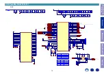


SCH04 SoundBar Main PCB MCU
g
TDI
GND
MCU_RESET
P1[3B], P4[2C]
4K7
0402
R347
GND
4K7
0402
R349
4K7
0402
R350
4K7
0402
R351
4K7
0402
R352
I2C3_SCL
P2[2C], P2[5B], P9[7C]
I2
C
3_
S
D
A
P
2[
2C
],
P
2[
5B
],
P
9[
6C
]
H
S
D
A
0
P
7[
6B
]
H
S
C
L
0
P
7[
6B
]
4K7
0402
R358
D
E
T
O
N
_A
N
A
L
O
G
P
3[
7C
]
V
O
L
+
P
1[
3C
],
P
7[
2B
]
V
O
L
-
P
1[
3C
],
P
7[
2B
]
M
U
T
E
P
1[
3C
],
P
7[
2B
]
H
D
M
I_
R
S
T
P
7[
6B
]
P
A
_R
E
S
E
T
P
9[
2B
],
P
9[
2D
]
N
IR
Q
1
P
7[
6B
]
N
IR
Q
A
0
P
10
[4
C
],
P
7[
6A
]
N
O
S
D
IR
Q
P
7[
6A
]
S
-E
R
R
_A
P
10
[3
B
],
P
2[
7B
]
S
-E
R
R
_B
P
10
[3
B
],
P
2[
3C
]
A
M
P
_P
D
N
P
9[
1A
],
P
9[
1C
]
C
M
_R
T
S
P
1[
7B
]
A
M
P
_F
A
U
L
T
P
9[
1A
],
P
9[
1C
]
DETON_OPT
P4[4C], P7[7B]
HCS
P7[6B]
HSCLK
P5[7B], P7[6B]
HMOSI
P5[7B], P7[6B]
HMISO
P5[7B], P7[6B]
DETON_COAX
P4[4C], P7[6B]
CM_CTS
P1[7B]
CM_TXD
P1[5B], P4[1C]
CM_RXD
P1[5B], P4[1B]
RCSCT
VCC
TDO
GND
UB
MD
EMLE
TRST
TCK
TMS
STBY_STATUS
P1[5B]
GND
GND
GND
GND
GND
3.3V_EVER
100nF
16V
C368
100nF
16V
C371
100nF
C376
600R@100MHz
L31
10
0n
F
C
37
9
3.3V_EVER
100nF
16V
C375
600R@100MHz
L33
GND
3.3V_EVER
100nF
16V
C365
600R@100MHz
L30
GND
100nF
16V
C369
100nF
16V
C367
S
P
I_
D
S
P
A
C
S
P
4[
8B
],
P
5[
7B
],
P
5[
8D
]
SPI_CLKA
P5[6D], P5[7B]
SPI_MISOA
P5[7B], P5[8D]
CM_SCK
P1[5B], P4[6B]
CM_MISO
P1[5B], P4[6B]
C
M
_M
O
S
I
P
1[
7B
],
P
4[
6B
]
GND
SPI_MOSIA
P5[6D], P5[7B]
CM_SSO
P1[5B]
SPI_DSPACS
P4[5B], P5[7B], P5[8D]
5.0V_EVER
GND
MCU_BTMD
P1[4A], P4[1B]
CEC_IN
P4[1B]
LMBT3904LT1G
SOT-23
1
3
2
Q17
DNI
16V
C364
GND
CEC_OUT
P4[3B]
CEC
P4[6C], P7[6B]
LMBT3904LT1G
SOT-23
1
3
2
Q19
LMBT3904LT1G
SOT-23
1
3
2
Q18
4K7
0402
R319
2.2M
0603
R317
GND
27K4
0402
R321
BAT54
D21
22R
R343
DNI
0402
R346
CEC
P4[1A], P7[6B]
DSPA_HOLD
P5[7B]
DSPA_BOOT
P5[7B]
DIST_MUTE
P2[3D]
NET_PW
P8[2C]
CEC_OUT
P4[1A]
HDMI_PW
P7[6A], P8[2A]
DSP_PW
P8[4D]
MCU_RESET
P1[3B], P4[3B]
100nF
16V
C381
GND
TDO
P4[2B], P4[2C]
TDO
P4[2B], P4[3C]
TDI
P4[2C]
TDI
P4[2C], P4[3C]
UBOOTEN
P4[2C]
UBOOTEN
P4[5D]
MD
P4[2B]
MD
P4[2C]
EMLE
P4[3B]
EMLE
P4[2C]
TRST
P4[3C]
TRST
P4[2C]
GND
RxD
TxD
GND
USBCNVRxD
P4[2D], P7[2C]
USBCNVTxD
P4[2D], P7[2C]
GND
SDA3
P9[1B], P9[1C]
SCL3
P9[1B], P9[1C]
GND
10K
0402
R312
GND
D
IR
_R
E
S
E
T
P
2[
1C
],
P
2[
5B
]
CH_MODE
P5[7B]
100nF
16V
C370
GND
1M
0402
R340
R
X
0_
D
E
T
P
7[
6B
]
H
P
D
_M
C
U
0
P
7[
6B
]
10K
0402
R325
10K
0402
R324
4K7
0402
R348
10K
0402
R357
100nF
16V
C374
SD A 3
D IST _MU T E
SCL 3
ST BY _ST A T U S
CE C
CM_ RX D
U A RT SCK IN
CM_ T X D
CM_ CT S
D SP1 _H O L D
D E T O N _CO A X
H MISO
H MO SI
H SCL K
H CS
D E T O N _O PT
D SP1 _BO O T /FIQ 1
D SP1 _H N D SK _1
CH _MO D E
CM_ MO SI
CM_ SCK
SPI_ SS
CM_ MISO
H
P
D
_M
C
U
3
D
IR
_
R
E
S
E
T
R
X
3_
D
E
T
H
D
M
IS
C
L
H
D
M
IS
D
A
I2
C
3_
S
D
A
U
B
I2C3 _SCL
CT S
T D O
FIN E C/T CK
T D I
T MS
U SBCN V T xD
U SBCN V Rx D
T RST
MCU _RE SE T
D SP_ PW
H D MI_ PW
CE C_ O U T
N E T _PW
E ML E
CE C_ IN
S
P
I_
D
S
P
A
C
S
C
M
_
R
T
S
A
M
P
_P
D
N
S
-E
R
R
_
B
S
-E
R
R
_
A
N
O
S
D
IR
Q
N
IR
Q
A
0
N
IR
Q
1
P
A
_R
E
S
E
T
H
D
M
I_
R
S
T
M
U
T
E
V
O
L
-
V
O
L
+
D
E
T
O
N
_
A
U
X
GND
CM_MISO
P1[5B], P4[6B]
SPI_SS
P5[7B]
CM_SCK
P1[5B], P4[6B]
CM_MOSI
P1[7B], P4[7C]
DSPA_HNDSK
P5[7B]
3.3V_EVER
1
TP105
100K
0402
R314
DSPARESET
P5[4C]
CEC_PW
P7[6B]
D SPA RE SE T
CE C_ PW
22R
R327
22R
R329
22R
R330
22R
R334
22R
R336
OR_DSPAI_SLx
Main input selector for DSP-A
000
001
010
011
1XX
PCM9211-A ADC(default)
PCM9211-A DIR
PCM9211-B DIR
LEGO I2S0
MN864788A Autio
B
T
_P
A
IR
P
1[
3B
],
P
7[
7B
]
B
T
_P
A
IR
C
O
N
N
E
C
T
P
1[
3C
],
P
7[
7B
]
T
X
0_
H
P
D
P
7[
6B
]
T
X
0_
H
P
D
4K7
R342
D
E
T
O
N
_C
O
A
X
P
4[
6B
],
P
7[
6B
]
D
E
T
O
N
_O
P
T
P
4[
6B
],
P
7[
7B
]
D
E
T
O
N
_C
O
A
X
D
E
T
O
N
_O
P
T
C
M
W
A
K
E
U
P
P
1[
8B
]
D
S
P
1_
F
M
T
_C
H
G
P
5[
7B
]
K
E
Y
IN
P
1[
3C
]
M
IC
_M
U
T
E
P
3[
6B
]
D
S
P
1_
F
M
T
_C
H
G
K
E
Y
IN
M
IC
_
M
U
T
E
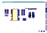
R5F5634BCDFB
AVSS
1
P05/DA1
2
VREFH
3
P03/DA0
4
VREFL
5
P02/IRQ10
6
P01/PMC1
7
P00/PMC0
8
PF5/IRQ4
9
EMLE
10
PJ5
11
VSS
12
PJ3/RTS0#
13
VCL
14
PJ1
15
MD/FINED
16
PJ2
17
PJ4
18
RES#
19
XTAL
20
VSS
21
EXTAL
22
VCC
23
P35/NMI
24
TRST#
25
P33/RXD0
26
P32/TXD0
27
TMS
28
TDI
29
FINEC/TCK
30
TDO
31
P25
32
P24/SCK3
33
P23/CTS0#
34
P22/SCK0
35
P21/SCL1
36
P
20
/S
D
A
1
37
P
17
/T
X
D
3
38
P
87
39
P
16
40
P
86
41
P
15
42
P
14
43
S
D
A
0
44
S
C
L
0
45
P
H
3
46
P
H
2
47
P
H
1
48
PC1/SDA3
73
PL1
74
PC0/SCL3
75
PL0
76
P73/CECIO
77
PB7/TXD9
78
PB6/RXD9
79
PB5/SCK9
80
PB4/RTS9#
81
PB3
82
PB2
83
PB1
84
P72
85
P71
86
PB0
87
PA7/MISOA
88
PA6/MOSIA
89
PA5/RSPCKA
90
VCC
91
PA4/SSLA0
92
VSS
93
PA3
94
PA2
95
PA1
96
PA0
97
P67
98
P66
99
P65
100
PE7
101
PE6/MOSIB
102
PK5/TXD4
103
P70
104
PK4/RXD4
105
PE5/RSPCKB
106
PE4/SSLB0
107
PE3/MISOB
108
P
H
0/
C
A
C
R
E
F
49
P
56
/T
X
D
2
50
P
55
51
P
54
/R
T
S
2#
52
P
53
53
P
52
/R
X
D
2
54
P
51
/S
C
K
2
55
T
X
D
2
56
V
S
S
57
P
83
58
V
C
C
59
P
C
7
60
P
C
6
61
P
C
5
62
P
82
63
P
81
64
P
80
65
P
C
4/
S
C
K
5
66
P
C
3/
T
X
D
5
67
P
77
/T
X
D
11
68
P
76
/R
X
D
11
69
P
C
2/
R
X
D
5
70
P
75
/S
C
K
11
71
P
74
72
P
E
2/
S
S
L
B
3
10
9
P
E
2/
S
S
L
B
2
11
0
P
E
0/
S
S
L
B
1
11
1
P
64
11
2
P
63
11
3
P
62
11
4
P
61
/C
T
S
9#
11
5
P
K
3
11
6
P
60
11
7
P
K
2
11
8
P
D
7
11
9
P
D
6/
IR
Q
6
12
0
P
D
5/
IR
Q
5
12
1
P
D
4/
IR
Q
4
12
2
P
D
3/
IR
Q
3
12
3
P
D
2/
IR
Q
2
12
4
P
D
1/
IR
Q
1
12
5
P
D
0/
IR
Q
0
12
6
P
93
12
7
P
92
12
8
P
91
12
9
V
S
S
13
0
P
90
13
1
V
C
C
13
2
P
47
/A
N
00
7
13
3
P
46
/A
N
00
6
13
4
P
45
/A
N
00
5
13
5
P
44
/A
N
00
4
13
6
P
43
/A
N
00
3
13
7
P
42
/A
N
00
2
13
8
P
41
/A
N
00
1
13
9
V
R
E
F
L
0
14
0
P
40
/A
N
00
0
14
1
V
R
E
F
H
0
14
2
A
V
C
C
0
14
3
P
07
14
4
U34
SN74CBT3257CPWR
S
1
1B1
2
1B2
3
1A
4
2B1
5
2B2
6
2A
7
G
N
D
8
P
F
5
9
3B2
10
3B1
11
4A
12
4B2
13
4B1
14
OE
15
V
C
C
16
U18
1
GND
2
3
GND
4
Y7
33R
R344
GND
GND
GND
LMBT3904LT1G
SOT-23
1
3
2
Q20
4K7
0402
R331
5.0V_EVER
GND
10K
0402
R337
10K
0402
R338
100K
R341
100K
R345
GND
GND
MCU_BTMD
P1[4A], P4[2B]
CM_RXD
P1[5B], P4[6C]
CM_TXD
P1[5B], P4[6C]
TDO
P4[2C], P4[3C]
TDI
P4[2C], P4[3C]
AC_FAULT
P4[2B]
AC_FAULT
P4[3B]
GND
3.3V_EVER
1SS355
D22
GND
HV
10nF
16V
C373
GND
GND
3.3V_EVER
33R
0402
R354
220R
R356
22R
0402
R353
1M
R355
GND
GND
GND
3.3VDCORE
100nF
16V
C380
GND
330K
0603
R359
3.3V_EVER
3
5
SN74AHC1GU04DCKRE4
2
4
VC C
GND
U33
SOT-323FL
RU1C001UNTCL
1
2
3
Q21
SOT-323FL
RU1C001UNTCL
1
2
3
Q22
SOT-323FL
RU1C001UNTCL
1
2
3
Q23
SOT-323FL
RU1C001UNTCL
1
2
3
Q24
BU45K442
V
C
C
3
G
N
D
1
RESET
2
U22
47K
0402
R335
9
10
8
SN74L VC08APW
U15C
0R
R316
GND
470K
0402
R323
1M
0402
R322
47pF
50V
C366
4.9152 MHz
1
2
Y4
TP103
TP102
TP100
TP92
TP101
TP94
TP95
TP104
TP99
TP98
TP97
TP96
33pF
50V
C378
33pF
50V
C377
680R
0402
R339
1
TP93
33pF
50V
C382
33pF
50V
C383
D
e_
em
ph
a
P
2[
3D
]
CAPC0603
2.2uF
6.3V
C372
MCU
3.3V_EVER
CEC_IN
P4[3B]
WOOFER_PAIR
P7[7B], P9[8C]
D83_RESET
P9[5D]
4
5
6
SN74L VC08APW
U15B
FIN E C/T CK
T MS
100R
0402
R361
10K
0402
R360
IR Sensor circuit
GND
100nF
16V
C384
GND
GND
10uF
6.3V
C387
1nF
50V
C386
10nF
C385
W0038S-6
GND
2
VCC
3
OUT
1
IR
3.3V_EVER
IR_IN
U SBCN V RT S
D
e_
em
ph
a
C
O
N
N
E
C
T
0R
R313
OR_MDACBP1
P10[3B]
O R_ MD A CBP1
O R_ MD A CBP0
OR_DSPAI_SL0
P10[3B]
OR_DSPAI_SL1
P10[3B]
OR_DSPAI_SL2
P10[3B]
O R_ D SPA I_SL 2
O R_ D SPA I_SL 1
O R_ D SPA I_SL 0
P
L
D
_T
M
S
P
1[
7B
],
P
10
[4
B
]
P
L
D
_T
C
K
P
1[
7B
],
P
10
[4
B
]
P
L
D
_T
M
S
P
L
D
_T
C
K
P
L
D
_T
D
I
P
1[
7B
],
P
10
[4
B
]
P
L
D
_T
D
O
P
L
D
_T
D
O
P
1[
7B
],
P
10
[4
C
]
P
L
D
_T
D
I
H
P
D
_M
C
U
2
H
P
D
_M
C
U
1
H
P
D
_M
C
U
0
M
D
A
C
_M
U
T
E
P
10
[5
A
]
M
D
A
C
_M
U
T
E
O
R
_S
D
A
C
_I
N
S
E
L
2
P
10
[3
B
]
O
R
_S
D
A
C
_I
N
S
E
L
1
P
10
[3
B
]
O
R
_S
D
A
C
_I
N
S
E
L
0
P
10
[3
B
]
P
L
D
_S
P
IL
T
P
10
[4
C
]
P
L
D
_S
P
IC
L
K
P
10
[3
B
]
P
L
D
_S
P
ID
A
T
A
P
L
D
_S
P
IC
L
K
P
L
D
_S
P
IL
T
O
R
_S
D
A
C
I_
S
L
0
O
R
_S
D
A
C
I_
S
L
1
N
O
M
_P
W
P
8[
4B
],
P
8[
6B
]
O
B
U
F
_Z
S
T
B
Y
P
10
[5
A
]
O
B
U
F
_Z
S
T
B
Y
S
R
E
M
O
T
E
_
R
X
D
N
O
M
_P
W
S
R
E
M
O
T
E
_
T
X
D
IN
T
1
P
L
D
_S
P
ID
A
T
A
P
10
[3
B
]
O
R
_S
D
A
C
I_
S
L
2
R
X
0_
D
E
T
R
X
1_
D
E
T
R
X
2_
D
E
T
IR_ IN
IRSIG_MCU
P4[3D]
IRSIG_MCU
P4[3B]
W
A
K
E
U
P
_M
O
D
U
L
E
-
7
+
14
1
2
3
SN74L VC08APW
U15A
DNI
R57
DNI
R63
DNI
R4
DNI
R62
A
M
P
_F
A
U
L
T
S
P
_P
R
O
T
E
C
T
P
9[
5A
]
D
C
_P
R
O
T
E
C
T
TP253
TP296
TP297
TP301
TP303
TP304
TP299
TP300
10K 0402
R277
10K 0402
R278
3.3V_EVER
10K 0402
R283
10K 0402
R286
3.3V_EVER
I2C3 _SCL
I2C3 _SD A
D83_EN
P9[6C]
D 83_E N
D 83_RE SE T
W O O FE R_ PA IR
HCS2
P5[7B]
H CS2
22R
R213
22R
R272
22R
R273
22R
R275
IR1_IN
P7[2C]
0R
R304
22K
0402
R320
U A RT SCK IN
USBCNVRxD
P4[2D], P4[3C]
USBCNVTxD
P4[2D], P4[3C]
DNI
1
2
3
4
5
6
7
J8
DNI
1
2
3
4
5
6
7
8
9
10
11
CN4
13K
R328
3K6
R333
51K
R332
10K
0402
R315
1%
0402
11K
R318
TP116
TP117
TP118
TP106
TP107
TP108
TP109
TP110
TP111
TP112
TP113
TP114
TP115
TP14
TP36
TP37
Ref
HEOSHCHS2
DHT-S516H
R315
10k
10k
R318
11k
24k
OPTION TABLE
※Use a tolerance of ± 1% (F product) for resistance.
Before Servicing
This Unit
Electrical
Mechanical
Repair Information
Updating
11


