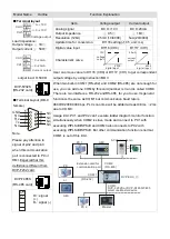

Model Name
Outline
Function Explanation
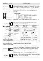
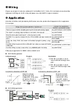
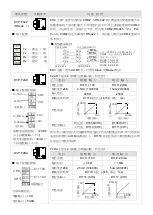
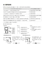
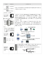
Terminal layout
V0+
I0+
V1+
I1+
COM
0~+10V
0~+10V
CH0
CH1
Voltage output
Load Impedance:
Output voltage
≧
1K
Ω
Output current
≦
500
Ω
V0+
I0+
V1+
I1+
COM
CH0
CH1
0~20mA
0~20mA
Current output
output load: 0~500Ω
Item
Voltage output
Current output
Analog signal
DC 0~+10V
DC 0~20mA
Output impedance
≦
0.5
Ω
≧
1M
Ω
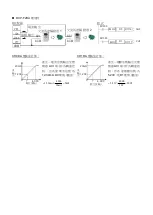
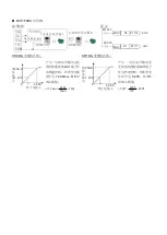
Resolution (12bit)
2.5mV (10/4000)
5uA (20/4000)
Update time for conversion
D1118 setting (
≧
K
5, unit: ms)
Digital value input
D1116 (CH0)
D1117 (CH1)
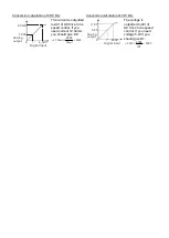
Characteristic curve
4000
10V
0
voltage
output
digital input
digital input
0
20mA
4000
current
output
User can move value to D1116 (CH0) or D1117 (CH1) to get correspondent
output voltage by using instruction MOV.
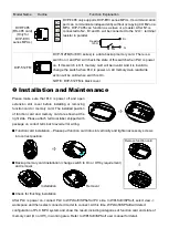
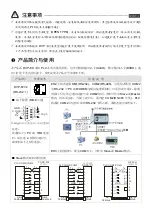
DVP-F232S
(RS-232 card)
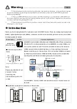
When two built-in COM1 (RS-232) and COM2 (RS-485) are not enough for
use, you can add one COM by this card (number is 3 and is called COM3.
There are two interfaces, RS-232 and RS-485, for you to use. Its general
function is the same as COM1 but communication baud rate is
9600/19200/38400 bps. PLC scan time will be added at least 0.8ms ~ 2ms
due to COM3.
Usage limit: PC1 and PC2 can’t execute ladder diagram monitor function
simultaneously when COM2 is slave mode and connect to PC1 with
executing WPLSoft/ISPSoft and COM3 also connects to PC2 with
executing WPLSoft/ISPSoft. But other communication function is normal.
COM1 is out of this limit.
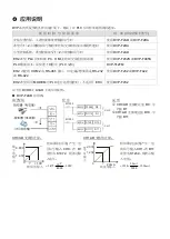
Master
PC 2
HMI
PC
PC 1
HMI
COM1
COM2
COM3
(RS-232)
(RS-485)
DVP-F232S or DVP-F485S/F485
DVP EH
MP U
AC drive or Servo
Extension card for
communication port
select one Master device
or
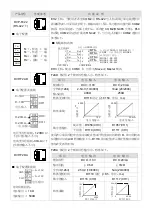
Terminal Layout (DB-9
female)
GND
Tx
Rx
5
3
2
1
9
8
7
6
4
NC
NC
NC
NC
NC
NC
Note:
Please pay attention to
signal of pin2 and pin3
when this communication
port is connected to PC or
HMI. Especial that this
definition is different from
DVP-F232 card.
DVP-F485S
(RS-485 card)
D+
D-
D+: signal
(+)
D-: signal (-)
Summary of Contents for DVP-EH Series
Page 1: ...DVP 0407730 01 20200727...