background image


DELTA ELECTRONICS, INC.


2 2007/11/6

Rev. 0D

www.deltaww.com


Absolute Maximum Ratings 

Parameter Symbol

Min. 

Typ. 

Max. 

Unit 

Note 

Storage Temperature 

Ts 

-40 


85 

ºC 


Supply Voltage 

V

CC

 0    5  V 


Recommended Operating Conditions 

Parameter Symbol

Min. 

Typ. 

Max. 

Unit 

Note 

Case Operating Temperature 
Commercial 
Extended 
Industrial 

T

C


-5 

-10 
-40 


70 
85 
85 

ºC 1 

Supply Voltage 

V

CC

 3.135

  3.465


Note 1: See order information 

Electrical Characteristics 

(V

CC

=3.135V to 3.465V) 

Parameter Symbol

Min. 

Typ. 

Max. 

Unit 

Note 

Total Supply Current 

I

CCT

    300 mA 


Transmitter 

Transmitter Differential Input Voltage 

V

DT


0.5  2.4  V 

Transmitter Disable Input-High 

V

DISH

2  

V

CC

+0.3

V  

Transmitter Disable Input-Low 

V

DISL

0  0.8 V 


Transmitter Fault Output-High 

V

TXFH

2  

V

CC

+0.3

V 3 

Transmitter Fault Output-Low 

V

TXFL

0  0.8 V 

Receiver 

Receiver Differential Output Voltage 

V

DR

 0.35 0.7  2 

LOS Output Voltage-High 

V

LOSH

2  

V

CC

+0.3

V 3 

LOS Output Voltage-Low 

V

LOSL

0  0.8 V 

Output Data Rise/Fall Time 

t

r

 / t

f


2.2 

nsec  5 

 
Notes: 

2.  Internally AC coupled and terminated to 100Ohm differential load. 

3.  Pull up to V

CC

 with a 4.7K – 10K Ohm resistor on host Board   

4.  Internally AC coupled, but requires a 100 Ohm differential termination at or internal to Serializer/ 

Deserializer. 

5.  These are 20%~80% values 

Summary of Contents for LCP-155A4HSRBx Series

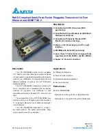
Page 1: ...ns that require rates of up to 155Mbit sec It is compliant with the Fast Ethernet standards as well as the SFP Multisource Agreement MSA The LCP 155A4HSRBx transceivers provide with the LC receptacle that is compatible with the industry standard LC connector The transceiver is also compatible with industry standard RFT connector and cage The post amplifier of the LCP 155A4HSRBx also includes a LOS...

Page 2: ...ransmitter Transmitter Differential Input Voltage VDT 0 5 2 4 V 2 Transmitter Disable Input High VDISH 2 VCC 0 3 V Transmitter Disable Input Low VDISL 0 0 8 V Transmitter Fault Output High VTXFH 2 VCC 0 3 V 3 Transmitter Fault Output Low VTXFL 0 0 8 V 3 Receiver Receiver Differential Output Voltage VDR 0 35 0 7 2 V 4 LOS Output Voltage High VLOSH 2 VCC 0 3 V 3 LOS Output Voltage Low VLOSL 0 0 8 V ...

Page 3: ...Spectral Width RMS σ 0 85 nm Optical Rise Fall Time tr tf 2 5 nsec 1 Total Jitter pk pk TJ 2 5 ns Transmitter eye mask definition X1 X2 X3 Y1 Y2 Y3 Y4 0 18 0 29 0 35 0 35 0 38 0 4 0 55 UI Receiver Sensitivity Avg PIN 25 dBm 2 Input Optical Wavelength λ 850 nm LOS De Asserted Avg PD 26 dBm LOS asserted Avg PA 38 dBm LOS Hysteresis PD PA 0 5 dB Overload PO 3 dBm Notes 1 These are 20 80 values 2 The ...

Page 4: ...al ID interface 6 MOD DEF0 Module Definition 0 3 Note 3 Grounded in Module 7 Rate Select Not Connect 3 Function not available 8 LOS Loss of Signal 3 Note 4 9 VeeR Receiver Ground 1 Note 5 10 VeeR Receiver Ground 1 Note 5 11 VeeR Receiver Ground 1 Note 5 12 RD Inv Received Data Out 3 Note 6 13 RD Received Data Out 3 Note 7 14 VeeR Receiver Ground 1 Note 5 15 VccR Receiver Power 2 3 3 5 Note 7 16 Vc...

Page 5: ...on In the low state the output will be pulled to 0 8V 5 VeeR and VeeT may be internally connected within the SFP module 6 RD These are the differential receiver outputs They are AC coupled 100Ω differential lines which should be terminated with 100Ω differential at the user SERDES The AC coupling is done inside the module and is thus not required on the host board The voltage swing on these lines ...

Page 6: ... 01uF 0 01uF 0 1uF 10uF RES1 RES1 100 Ohms RES1 RES1 RES1 10k Ohms 100 Ohms VCC Protocol Vcc SerDes IC Protocol IC PLD PAL Mod_def 2 Mod_def 1 Mod_def 0 3 3V 3 3V DELTA SFP Module Preamp Tx_Disable Quantizer Tx_Fault TD TD VeeT RD RD Rx_LOS VeeR Tx_Disable Tx_Fault Rx_LOS RES1 4 7k to 10k Ohms VccT VccR Laser Driver Depands on SerDes IC used EEPROM ...

Page 7: ...DELTA ELECTRONICS INC 7 2007 11 6 Rev 0D www deltaww com Package Outline Drawing for Metal Housing with Bail de latch Latch Color Identifier Black Complies with 21 CFR 1040 10 and 1040 11 Made in x FS ...

Page 8: ...ABLE to when the modulated optical output rises above 90 of nominal Time to initialize including reset of TX_FAULT t_init 300 msec From power on or negation of TX_Fault using TX Disable TX Fault Assert Time t_fault 100 µsec Time from fault to TX fault on TX_DISABLE to reset t_rest 10 µsec Time TX Disable must be held high to reset TX_Fault LOS Assert Time t_loss_on 100 µsec Time from LOS state to ...

Page 9: ... SFP TX_DISABLE asserted Initialization during hot plugging of SFP TRANSCEIVER Example of initialization during hot plugging TX_DISABLE negated SFP TX_DISABLE timing during normal operation Detection of transmitter safety fault condition Successful recovery from transient safety fault condition Unsuccessful recovery from safety fault condition Timing of LOS detection ...

Page 10: ... 108 00 09 00 34 20 59 20 84 DC Note 3 109 00 10 00 35 20 60 03 85 DC 110 00 11 03 36 00 61 52 86 DC 111 00 12 01 37 00 62 00 87 DC 112 00 13 00 38 00 63 CS1 Note 1 88 DC 113 00 14 00 39 00 64 00 89 DC 114 00 15 00 40 4C L 65 1A 90 DC 115 00 16 C8 41 43 C 66 00 91 DC 116 00 17 64 42 50 P 67 00 92 00 117 00 18 00 43 2D 68 SN Note 2 93 00 118 00 19 00 44 31 1 69 SN 94 00 119 00 20 44 D 45 35 5 70 SN...

Page 11: ...ical Pins MIL STD 883E Method 3015 7 1 Satisfied with electrical characteristics of product spec 2 No physical damage Eye Safety US FDA CDRH AEL Class 1 EN 60950 2000 EN 60825 1 1994 A11 A2 EN 60825 2 2000 CDRH File 0321539 00 TUV Certificate No R50032471 Component Recognition Underwriters Laboratories and Canadian Standards Association Joint Component Recognition for Information Technology Equipm...

Page 12: ...te Contents 0A Sep 2007 Preliminary Datasheet 0B Oct 16 2007 Modified the Byte6 of A0h from 00h to 20h Add the total jitter specification of TX 0C Oct 23 2007 Add latch color identifier Modify the Byte5 Byte6 Byte11 and Byte12 of A0h 0D Nov 06 2007 Modify the Byte 12 from 02h to 01h ...

Reviews: