background image


DS_DNM04SMD10_07162008 

12


FEATURE DESCRIPTIONS (CON.


Sequential Start-up 

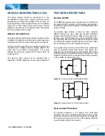
Sequential start-up (Figure 40) is implemented by placing 
an On/Off control circuit between Vo

PS1

 and the On/Off pin 

of PS2.   


Simultaneous 

Simultaneous tracking (Figure 41) is implemented by 
using the TRACK pin. The objective is to minimize the 
voltage difference between the power supply outputs 
during power up and down.   


The simultaneous tracking can be accomplished by 
connecting Vo

PS1

 to the TRACK pin of PS2. Please note 

the voltage apply to TRACK pin needs to always higher 
than the Vo

PS2

 set point voltage. 


R1

R2

Vo

PS1

PS1

Vin

On/Off

On/Off

PS2

Vo

PS2

Vin

C1

Q1

R3

TRACK

Vo

PS1

PS2

Vo

PS2

PS1

Vin

Vin

On/Off

On/Off

Summary of Contents for 0.75-3.3V

Page 1: ...e On Off logic Tracking feature SIP package Delphi DNM Non Isolated Point of Load DC DC Power Modules 2 8 5 5Vin 0 75 3 3V 10Aout The Delphi Series DNM 2 8 5 5V input single output non isolated Point...

Page 2: ...Current Hiccup Mode Io s c 3 5 Adc DYNAMIC CHARACTERISTICS Dynamic Load Response 10 F Tan 1 F Ceramic load cap 2 5A s Positive Step Change in Output Current 50 Io max to 100 Io max 200 mV Negative St...

Page 3: ...ent 0 75V out 75 80 85 90 95 100 1 2 3 4 5 6 7 8 9 10 OUTPUR CURRENT A EFFICIENCY Vin 5 0V Vin 4 5V Vin 5 5V 75 80 85 90 95 100 1 2 3 4 5 6 7 8 9 10 OUTPUR CURRENT A EFFICIENCY Vin 5 0 Vin 3 0V Vin 5...

Page 4: ...ise at 3 3Vin 2 5V 10A out Figure 8 Output ripple noise at 3 3Vin 1 8V 10A out Figure 9 Output ripple noise at 5Vin 3 3V 10A out Figure 10 Output ripple noise at 5Vin 1 8V 10A out Figure 11 Turn on de...

Page 5: ...1 8V 10A out Figure 15 Turn on delay time at remote turn on 5Vin 3 3V 16A out Figure 16 Turn on delay time at remote turn on 3 3Vin 2 5V 16A out Figure 17 Turn on delay time at remote turn on with ext...

Page 6: ...ypical Transient Response to Step Load Change at 2 5A S from 100 to 50 of Io max at 5Vin 1 8Vout Cout 1uF ceramic 10 F Tantalum Figure 22 Typical Transient Response to Step Load Change at 2 5A S from...

Page 7: ...rom 100 to 50 of Io max at 3 3Vin 1 8Vout Cout 1uF ceramic 10 F Tantalum Figure 26 Typical Transient Response to Step Load Change at 2 5A S from 50 to 100 of Io max at 3 3Vin 1 8Vout Cout 1uF ceramic...

Page 8: ...Vo DESIGN CONSIDERATIONS To maintain low noise and ripple at the input voltage it is critical to use low ESR capacitors at the input to the module Figure 32 shows the input ripple voltage mVp p for v...

Page 9: ...itive and negative On Off logic options are available in the DNM DNL series power modules For positive logic module connect an open collector NPN transistor or open drain N channel MOSFET between the...

Page 10: ...ins of the module Without this external resistor the output voltage of the module is 0 7525 Vdc To calculate the value of the resistor Rtrim for a particular output voltage Vo please use the following...

Page 11: ...rim Q2 Q1 Rmargin up Rmargin down Rtrim Figure 39 Circuit configuration for output voltage margining Voltage Tracking The DNM family was designed for applications that have output voltage tracking req...

Page 12: ...implemented by using the TRACK pin The objective is to minimize the voltage difference between the power supply outputs during power up and down The simultaneous tracking can be accomplished by conne...

Page 13: ...rcuit cards in cabinet racks in which the power modules are mounted The following figure shows the wind tunnel characterization setup The power module is mounted on a test PWB and is vertically positi...

Page 14: ...emperature Output Current A Natural Convection Figure 46 DNM04S0A0S10 Standard Output Current vs Ambient Temperature and Air Velocity Vin 5V Vo 0 75V Either Orientation DNM04S0A0S10 Standard Output Cu...

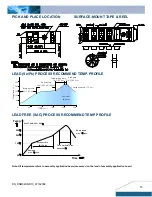
Page 15: ...erature C 50 100 150 200 250 300 60 0 120 180 240 2nd Ramp up temp 1 0 3 0 C sec Over 200 C 40 50sec Cooling down rate 3 C sec LEAD FREE SAC PROCESS RECOMMEND TEMP PROFILE Note All temperature refers...

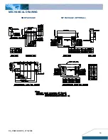
Page 16: ...DS_DNM04SMD10_07162008 16 MECHANICAL DRAWING SMD PACKAGE SIP PACKAGE OPTIONAL...

Page 17: ...dc 10A 96 0 CONTACT www delta com tw dcdc USA Telephone East Coast 888 335 8201 West Coast 888 335 8208 Fax 978 656 3964 Email DCDC delta corp com Europe Phone 41 31 998 53 11 Fax 41 31 998 53 53 Emai...

Reviews: