A-1
014–001867
Appendix A
VME Backplane Connector
Signals and Power Distribution
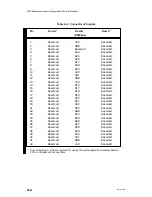
This appendix describes the VME connector signals J1 and J2; it also describes the
power signals the VME backplane receives from your computer’s power supply.
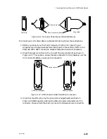
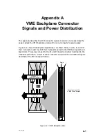
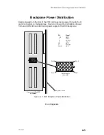
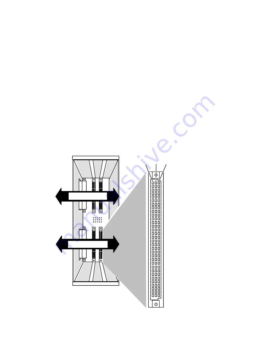
Figure A–1 shows the backplane signal buses. As shown below, rows A, B, and C of
the J1 connectors and row B of the J2 connectors provide the VMEbus signals to all
board slots. These rows connect to the P1 and P2 board connectors described in the
VMEbus specification. Row B of the J2 connectors provides the user-defined signals
described in the VMEbus specification.
Typical pin layout for
J1 and J2 connectors
VMEbus P1
(rows A, B, and C)
Rows
A
B
C
VMEbus P2
(row B)
Figure A–1 VME Backplane Bus
Summary of Contents for AViiON 5000 Series
Page 2: ......
Page 6: ......
Page 12: ...Preface x 014 001867 ...
Page 86: ...Configuring VME Option Boards 2 52 014 001867 ...
Page 144: ...Connecting External Devices to VME Option Boards 4 44 014 001867 ...
Page 150: ...VME Backplane Connector Signals and Power Distribution A 6 014 001867 ...
Page 196: ...Assigning VME Data Bus and Interrupt Priorities E 10 014 001867 ...
Page 206: ......
Page 210: ...Appendix Title ...

