background image

Enhanced FM Synthesizer Instruction Manual

IM10-OS3AH

4

This Page Intentionally Left Blank

Summary of Contents for OSR-3H061

Page 1: ...erved No part of this publication may be reproduced stored in a retrieval system or transmitted in any form or by any means electronic mechanical photocopying recording or otherwise without the prior...

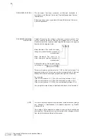
Page 2: ...igni cance of a revision Each element of the revision number signi es the scope of change as described in the diagram below DOCUMENT REVISION DEFINITION Major Revisions The result of a major change to...

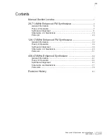
Page 3: ...eration 7 Synthesizer Alignment 11 Schematics and Illustrations 15 Parts List 23 128 174MHz Enhanced FM Synthesizer Enhanced FM Synthesizer Enhanced FM Synthesizer 31 General Information 33 Theory of...

Page 4: ...Enhanced FM Synthesizer Instruction Manual IM10 OS3AH iv This Page Intentionally Left Blank...

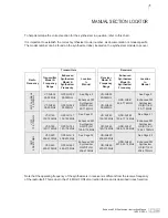
Page 5: ...38MHz OSR 3H061 50 4 71 4MHz See Page 3 Enhanced FM Synthesizer OS R T 3H 29 71 4MHz VT 3H045 38 50MHz OST 3H045 38 50MHz VR 3H045 38 50MHz VHF 132 174MHz VT 3 140 132 150MHz OST 3H141 132 150MHz See...

Page 6: ...Enhanced FM Synthesizer Instruction Manual IM10 OS3AH 2 This Page Intentionally Left Blank...

Page 7: ...MHz OST 3H045 38 50MHz VR 3H045 38 50MHz VHF 132 174MHz VT 3 140 132 150MHz OST 3H141 132 150MHz See Page 31 Enhanced FM Synthesizer OS R T 3H 128 6 174MHz VR 3H140 132 150MHz OSR 3H162 153 4 171 4MHz...

Page 8: ...Enhanced FM Synthesizer Instruction Manual IM10 OS3AH 4 This Page Intentionally Left Blank...

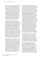
Page 9: ...minate residual electrical noise between digital and analog circuitry Further shielding of the synthesizer s RF lter circuitry is provided by an internal shielded enclosure GENERAL INFORMATION OS R T...

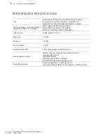
Page 10: ...ackets 29MHz 38MHz 0 5MHz OST 3H035 38MHz 50MHz 1 0MHz OST 3H045 50 4MHz 71 4MHz 1 0MHz OSR 3H061 Output Power 5dBm 2dBm into 50 Harmonics 30 dBc Spurious 90 dBc Hum and Noise 55 dB Modulation Sensiti...

Page 11: ...nals The analog board s main power is turned on and off by driving the optical receiver U1 U1 is driven by U4 on the digital board which is controlled by the microcontroller The main power regulators...

Page 12: ...y eliminates output harmonics SMB connector J2 provides interconnection to the companion transmitter or receiver with an output level of 5dBm 2dBm The 9 6 or 10 0MHz reference source is divided down t...

Page 13: ...s straightforward If all four of the CHANNEL SELECT lines CHAN SEL3 CHAN SEL0 are pulled low to GND the synthesizer will scan the four BCD switches FSW1 FSW4 located on the receiver or transmitter mai...

Page 14: ...d The channel number determines where the channel code number is retrieved from channel 1 is stored by the BCD switches and channels 2 through 16 are stored in the synthesizer s memory To calculate th...

Page 15: ...n ordinary soldering iron but should only be performed at surface mount rework and repair stations equipped with Electrostatic Discharge ESD protection When removing Surface Mount Solder Jumpers it is...

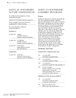
Page 16: ...ternal reference option is enabled This step is described in Reference Frequency Alignment in this section A change in operating frequency from the initial factory setting that exceeds the synthesizer...

Page 17: ...er board connection wires Attempt to maintain the position of the three inter board wires in order to simplify re assembly The digital board may now be extracted by removing four M2 machine screws Fol...

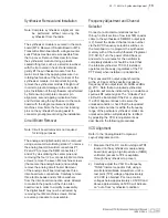
Page 18: ...CXO is adjusted Note this adjustment is only valid when the internal reference is selected JU1 in the B position on the analog board To adjust the internal TCXO referency frequency adjust the synthesi...

Page 19: ...n in which the last two digits of the circuit board number represent the circuit board version All PCB s manufactured by Daniels Electronics Ltd are identi ed by one of the following numbering convent...

Page 20: ...PLL FILTER FINE FREQUENCY ADJUST DIRECT LOW FREQUENCY MODULATION INPUT OPTIONAL HIGH STABILITY EXTERNAL REFERENCE A B ENHANCED BUFFER AMPLIFIER INTERNAL EXTERNAL REFERENCE INTERNAL FREQUENCY REFERENC...

Page 21: ...C10 A2 T C11 C2 T C12 E1 T C13 D1 T C14 A2 T C15 D1 T C16 A1 T C17 A3 T C18 B2 T C19 E2 T C20 D2 T C21 D2 T C22 D2 T C23 A4 T C24 B4 B C25 A4 T C26 C2 T C27 C1 T C28 B5 T C29 D3 T C30 D3 T C31 D3 T C...

Page 22: ...T C35 C5 T C36 C4 T C37 E4 B C38 E4 B C39 E4 B C40 B4 T C41 C5 T C42 E4 T C43 D4 T C44 C4 T C45 D4 B C46 E5 T C47 C4 T C48 A3 B C49 D3 B C50 D5 T C51 D5 T C52 E5 T C53 E5 T C54 D3 T C55 C4 T C56 C3 T...

Page 23: ...E U12 U14 J2 JU10 TCXO1 TP4 Q5 P3 R56 RV1 L13 LED1 C60 03 50038 03 OSx 3H061 OSx 3H045 OSx 3H035 PRODUCT FREQUENCY BAND IDENTIFICATION A B COLIN GUNN 24 FEB 97 C64 TP4 LOOP CONTROL SET FOR 2 3 VDC A B...

Page 24: ...4 B U2 B4 B U3 A1 B U4 A2 B U5 C4 B U6 C3 B U7 C3 B U8 C3 B U9 C2 B X1 C2 B A OS R T 3H 29 71 4MHZ DIGITAL BOARD COMPONENT LAYOUT BOTTOM DATE 25 MAR 96 TITLE OS R T 3 A H DIGITAL BOARD COMPONENT LAYOU...

Page 25: ...10 27K4 R27 27K4 R34 27K4 R35 27K4 R36 BC817 Q11 27K4 R22 27K4 R37 27K4 R13 100nF C9 BC817 Q3 27K4 R2 BC817 Q1 BC817 Q2 1 2 3 BC817 Q4 BC817 Q5 BC817 Q6 ENB CLK DIN LOCK DIN PWCTL OUTPUT SENSE 5VTAP F...

Page 26: ...Enhanced FM Synthesizer Instruction Manual IM10 OS3AH 22 This Page Intentionally Left Blank...

Page 27: ...1008 4A103K5R C10 CAP SM 100nF CER 0805 X7R 50 1008 5A104K5R C11 CAP SM 1 0uF TANT 20 16V 1055 5A105M16 C12 CAP SM 4 7uF TANT 10 16V 1055 5B475K16 C13 CAP SM 4 7uF TANT 10 16V 1055 5B475K16 C14 CAP SM...

Page 28: ...MK5 10 50V 1016 6D105K50 C39 CAP 1 0uF FILM MMK5 10 50V 1016 6D105K50 C40 CAP SM 33pF CER 0805 C0G 1008 1A330J1G C41 CAP SM 1nF CER 0805 X7R 50V 1008 3A102K5R C42 CAP SM 4 7uF TANT 10 16V 1055 5B475K1...

Page 29: ...51 4A00100K L5 INDUCTOR 9 5T 138nH MOLD WHT 1253 A0951389 L5 INDUCTOR 11 5T 197nH MOLD BRN 1253 A1151971 L5 INDUCTOR 13 5T 260nH MOLD ORG 1253 A1352603 L6 CHOKE RF MOLDED 10uH 10 25 1251 4A00100K L7 C...

Page 30: ...0805 1 100ppm 1150 4A1002FP R19 RES SM 10K0 0805 1 100ppm 1150 4A1002FP R20 RES SM 10R0 0805 1 100ppm 1150 1A10R0FP R21 RES SM 20K0 0805 1 100ppm 1150 4A2002FP R22 RES SM 1K00 0805 1 100ppm 1150 3A10...

Page 31: ...SM 18R2 0805 1 100ppm 1150 1A18R2FP R55 RES SM 274R 0805 1 100ppm 1150 2A2740FP R56 RES SM 274R 0805 1 100ppm 1150 2A2740FP RV1 POT SM 4mm SQ 5K SINGLE TURN 1174 AS2502J1 TCXO1 TCVCXO SMT 10MHz 1ppm 0...

Page 32: ...NG SOT23 2100 BAS16000 D2 DIODE BAS16 SWITCHING SOT23 2100 BAS16000 D3 DIODE BAS16 SWITCHING SOT23 2100 BAS16000 D4 DIODE BAS16 SWITCHING SOT23 2100 BAS16000 L1 INDUCTOR SM 10 0uH 10 1812 1255 4G10000...

Page 33: ...RES SM 215R 0805 1 100ppm 1150 2A2150FP R31 RES SM 215R 0805 1 100ppm 1150 2A2150FP R32 RES SM 215R 0805 1 100ppm 1150 2A2150FP R33 RES SM 332R 0805 1 100ppm 1150 2A3320FP R34 RES SM 27K4 0805 1 100pp...

Page 34: ...NGE 5120 J2SC01BG 2 FERRITE BEAD 43MIX 3x3 5mm OD 1210 43030350 3 LID CASE OS 3H SYNTH MODL AL 3702 66100921 1 PIN 2 x 10mm GROOVED W PILOT 5876 D1470210 4 SCREW M2 X 4 PAN PHILLIPS A2 5812 2M0PP04S 1...

Page 35: ...MHz VT 3H045 38 50MHz OST 3H045 38 50MHz VR 3H045 38 50MHz VHF 132 174MHz VT 3 140 132 150MHz OST 3H141 132 150MHz Enhanced FM Synthesizer OS R T 3H 128 6 174MHz VR 3H140 132 150MHz OSR 3H162 153 4 17...

Page 36: ...Enhanced FM Synthesizer Instruction Manual IM10 OS3AH 32 This Page Intentionally Left Blank...

Page 37: ...minate residual electrical noise between digital and analog circuitry Further shielding of the synthesizer s RF lter circuitry is provided by an internal shielded enclosure OS R T 3H ENHANCED SYNTHESI...

Page 38: ...brackets 128 6MHz 152 6MHz 2 0MHz OST 3H141 OSR 3H141 150MHz 174MHz 2 0MHz OST 3H162 OSR 3H162 Output Power 5dBm 2dBm into 50 Harmonics 30 dBc Spurious 90 dBc Hum and Noise 55 dB Modulation Sensitivi...

Page 39: ...d s main power is turned on and off by driving the optical receiver U1 U1 is driven by U4 on the digital board which is controlled by the microcontroller The main power regulators are provided by U6 a...

Page 40: ...iver with an output level of 5dBm 2dBm The 9 6 or 10 0MHz reference source is divided down to establish a channel selection step size of 5 0 6 25 2 5kHz A third order passive loop lter comprised of C3...

Page 41: ...cations but may be programmed in the eld using Daniels Synthesizer Channel Programmer CP SC 3 In transmitters the synthesizer operating frequency is the transmitter operating frequency For receivers...

Page 42: ...e channel code number is retrieved from channel 1 is stored by the BCD switches and channels 2 through 16 are stored in the synthesizer s memory To calculate the operating frequency for the OS R T 3H...

Page 43: ...n ordinary soldering iron but should only be performed at surface mount rework and repair stations equipped with Electrostatic Discharge ESD protection When removing Surface Mount Solder Jumpers it is...

Page 44: ...ve regulator output U6 positive regulator output TP2 5 0 0 1VDC U7 positive regulator output U7 positive regulator output TP3 5 0 0 1VDC U8 positive regulator output always on always on TP4 PLL error...

Page 45: ...the three inter board wires in order to simplify re assembly The digital board may now be extracted by removing four M2 machine screws Follow a reverse procedure to re assemble Frequency Adjustment a...

Page 46: ...le must be removed to change jumper JU2 on the digital board Note Care must be exercised when reinstalling the synthesizer module on the Transmitter Main board or the IF Audio board Pay careful attent...

Page 47: ...n in which the last two digits of the circuit board number represent the circuit board version All PCB s manufactured by Daniels Electronics Ltd are identi ed by one of the following numbering convent...

Page 48: ...TER FINE FREQUENCY ADJUST DIRECT LOW FREQUENCY MODULATION INPUT OPTIONAL HIGH STABILITY EXTERNAL REFERENCE A B ENHANCED BUFFER AMPLIFIER INTERNAL EXTERNAL REFERENCE INTERNAL FREQUENCY REFERENCE A DATE...

Page 49: ...al boards Remove seven M2 0 machine screws to remove analog board P2 P1 P3 LOCK DETECT LED J1 J2 TX RX 141 162 A B C D E 6 5 4 3 2 1 R22 0R0 Receiver 128 174 MHz OSR 3Hxxx Transmitter 128 174 MHz OST...

Page 50: ...1 5 H L10 1 5 H L2 10 H R51 220R R50 180R R40 180R C45 SEL L7 1 5 H C24 1 14pF C37 1 5 F C39 1 5 F L1 10 H R2 330R C38 SEL C49 SEL R36 R32 R33 SEL 1K2 SEL L9 1 5 H Q5 J211 L5 L3 10uH VHF LOW BAND 128...

Page 51: ...8VA SUPPLY POINTS EXTERNAL REFERENCE INPUT 50 FREQ CONTROL TCXO MOD INPUT 9 5 VDC SUPPLY TO ALL 5VA SUPPLY POINTS NC NC REFOUT LD R V VPD PDOUT GND RX TEST 1 FIN REFIN DIN CLK ENB OUTPUTA OUTPUTB VDD...

Page 52: ...4 B U3 A1 B U4 A2 B U5 C4 B U6 C3 B U7 C3 B U8 C3 B U9 C2 B X1 C2 B A OS R T 3H 128 174MHZ DIGITAL BOARD COMPONENT LAYOUT BOTTOM DATE 25 MAR 96 TITLE OS R T 3 A H DIGITAL BOARD COMPONENT LAYOUT TOP BO...

Page 53: ...R27 27K4 R34 27K4 R35 27K4 R36 BC817 Q11 27K4 R22 27K4 R37 27K4 R13 100nF C9 BC817 Q3 27K4 R2 BC817 Q1 BC817 Q2 1 2 3 BC817 Q4 BC817 Q5 BC817 Q6 ENB CLK DIN LOCK DIN PWCTL OUTPUT SENSE 5VTAP FB INPUT...

Page 54: ...Enhanced FM Synthesizer Instruction Manual IM10 OS3AH 50 This Page Intentionally Left Blank...

Page 55: ...0V 1008 4A103K5R C10 CAP SM 100nF CER 0805 X7R 50 1008 5A104K5R C11 CAP SM 1 0uF TANT 20 16V 1055 5A105M16 C12 CAP SM 4 7uF TANT 10 16V 1055 5B475K16 C13 CAP SM 4 7uF TANT 10 16V 1055 5B475K16 C14 CAP...

Page 56: ...SM 12pF CER 0805 C0G 1008 1A120J1G C42 CAP SM 22uF TANT 20 20V 1055 6D226M20 C43 CAP SM 10nF CER 0805 X7R 50V 1008 4A103K5R C44 CAP SM 330pF CER 0805 C0G 1008 2A331J1G C45 CAP 100nF FILM MMK5 10 63V...

Page 57: ...BC817025 Q2 TRANSISTOR BC817 25 NPN SOT23 2120 BC817025 Q3 TRANSISTOR BC807 25 PNP SOT23 2120 BC807025 Q4 TRANSISTOR BC817 25 NPN SOT23 2120 BC817025 Q5 JFET J211 RF N CHAN TO 92 2041 J2110000 R1 RES...

Page 58: ...S SM 10K0 0805 1 100ppm 1150 4A1002FP R35 RES SM 1K00 0805 1 100ppm 1150 3A1001FP R36 RES 2K2 METAL FILM 5 0 5W 1101 3A0222JP R36 RES 3K3 METAL FILM 5 0 5W 1101 3A0332JP R37 RES SM 10R0 0805 1 100ppm...

Page 59: ...SOR TTL O P PLST 2014 1L18230T U2 DIODE I R SENSOR TTL O P PLST 2014 1L18230T U3 DIODE I R SENSOR TTL O P PLST 2014 1L18230T U4 DIODE I R SENSOR TTL O P PLST 2014 1L18230T U5 LED I R GaAs 81 x 23 PLAS...

Page 60: ...ING SOT23 2100 BAS16000 D2 DIODE BAS16 SWITCHING SOT23 2100 BAS16000 D3 DIODE BAS16 SWITCHING SOT23 2100 BAS16000 D4 DIODE BAS16 SWITCHING SOT23 2100 BAS16000 L1 INDUCTOR SM 10 0uH 10 1812 1255 4G1000...

Page 61: ...RES SM 215R 0805 1 100ppm 1150 2A2150FP R31 RES SM 215R 0805 1 100ppm 1150 2A2150FP R32 RES SM 215R 0805 1 100ppm 1150 2A2150FP R33 RES SM 332R 0805 1 100ppm 1150 2A3320FP R34 RES SM 27K4 0805 1 100p...

Page 62: ...ANGE 5120 J2SC01BG 2 FERRITE BEAD 43MIX 3x3 5mm OD 1210 43030350 3 LID CASE OS 3H SYNTH MODL AL 3702 66100921 1 PIN 2 x 10mm GROOVED W PILOT 5876 D1470210 4 SCREW M2 X 4 PAN PHILLIPS A2 5812 2M0PP04S...

Page 63: ...29 71 4MHz VT 3H045 38 50MHz OST 3H045 38 50MHz VR 3H045 38 50MHz VHF 132 174MHz VT 3 140 132 150MHz OST 3H141 132 150MHz See Page 31 Enhanced FM Synthesizer OS R T 3H 128 6 174MHz VR 3H140 132 150MHz...

Page 64: ...Enhanced FM Synthesizer Instruction Manual IM10 OS3AH 60 This Page Intentionally Left Blank...

Page 65: ...minate residual electrical noise between digital and analog circuitry Further shielding of the synthesizer s RF lter circuitry is provided by an internal shielded enclosure OS R T 3H ENHANCED SYNTHESI...

Page 66: ...406MHz 430MHz Full Band OST 3H418 427 4MHz 451 4MHz Full Band OST 3H440 450MHz 470MHz Full Band OST 3H460 Output Power 5dBm 2dBm into 50 Harmonics 30 dBc Spurious 90 dBc Hum and Noise 55 dB Modulation...

Page 67: ...d s main power is turned on and off by driving the optical receiver U1 U1 is driven by U4 on the digital board which is controlled by the microcontroller The main power regulators are provided by U6 a...

Page 68: ...of the desired channel frequency In a transmitter the loss of lock will prevent a PTT from keying the power ampli er module thus preventing the transmission of a spurious output signal Adjusting capa...

Page 69: ...raightforward If all four of the CHANNEL SELECT lines CHAN SEL3 CHAN SEL0 are pulled low to GND the synthesizer will scan the four BCD switches FSW1 FSW4 located on the receiver or transmitter main bo...

Page 70: ...4 451 4MHz 427 4MHz 12 5kHz 12 5kHz Channelization The operating frequency for Synthesizers having 12 5kHz channelization is determined as follows BCD switch settings from 0000 to 4999 Multiply the s...

Page 71: ...n ordinary soldering iron but should only be performed at surface mount rework and repair stations equipped with Electrostatic Discharge ESD protection When removing Surface Mount Solder Jumpers it is...

Page 72: ...requency the internal reference option is enabled This step is described in Reference Frequency Alignment in this section A change in operating frequency from the initial factory setting that exceeds...

Page 73: ...digital board may now be extracted by removing four M2 machine screws Follow a reverse procedure to re assemble Frequency Adjustment and Channel Selection Connect a radio communications test set thro...

Page 74: ...should be made at room temperature 25 C after a ten minute stabilization period JUMPER CONFIGURATION The synthesizer s surface mount solder jumpers are clearly marked on both of it s digital and anal...

Page 75: ...n in which the last two digits of the circuit board number represent the circuit board version All PCB s manufactured by Daniels Electronics Ltd are identi ed by one of the following numbering convent...

Page 76: ...LL FILTER FINE FREQUENCY ADJUST DIRECT LOW FREQUENCY MODULATION INPUT OPTIONAL HIGH STABILITY EXTERNAL REFERENCE A B ENHANCED BUFFER AMPLIFIER INTERNAL EXTERNAL REFERENCE INTERNAL FREQUENCY REFERENCE...

Page 77: ...33R2 R52 Not Installed 49R9 MC145202F or MC145193F MC145190 U10 COMPONENT SELECTION TABLE TX 406 430 MHz band only JU4 SELECTION TABLE DESIG JU4 NOT INSTALLED RAKON IVT210BE 10 0 MHz SARONIX S2045 9 6...

Page 78: ...8 B3 T R49 B4 T R50 E5 B R51 D3 B R52 B3 T R53 B2 T R54 A6 T R55 B6 T R56 A6 T C42 B5 T C43 B5 T C44 A3 T C45 D3 B C46 B5 T C47 B3 T C49 D5 B C50 A5 T C51 A4 T C52 A5 T C53 A6 T C54 B4 T C55 B4 T C56...

Page 79: ...GRAM R58 RV1 U17 DATE 23 MAY 96 D5 UNUSED REFERENCE DESIGNATORS HIGHEST REFERENCE DESIGNATORS RF OUTPUT 3 5 dB Pad LOCK DETECT OUTPUT ACTIVATED WHEN UNLOCKED NC NC NC MODULATION INPUT POWER CNTRL ID 1...

Page 80: ...B U2 B4 B U3 A1 B U4 A2 B U5 C4 B U6 C3 B U7 C3 B U8 C3 B U9 C2 B X1 C2 B A OS R T 3H 406 470MHZ DIGITAL BOARD COMPONENT LAYOUT BOTTOM DATE 25 MAR 96 TITLE OS R T 3 A H DIGITAL BOARD COMPONENT LAYOUT...

Page 81: ...27K4 R27 27K4 R34 27K4 R35 27K4 R36 BC817 Q11 27K4 R22 27K4 R37 27K4 R13 100nF C9 BC817 Q3 27K4 R2 BC817 Q1 BC817 Q2 1 2 3 BC817 Q4 BC817 Q5 BC817 Q6 ENB CLK DIN LOCK DIN PWCTL OUTPUT SENSE 5VTAP FB...

Page 82: ...Enhanced FM Synthesizer Instruction Manual IM10 OS3AH 78 This Page Intentionally Left Blank...

Page 83: ...008 4A103K5R C10 CAP SM 100nF CER 0805 X7R 50 1008 5A104K5R C11 CAP SM 1 0uF TANT 20 16V 1055 5A105M16 C12 CAP SM 4 7uF TANT 10 16V 1055 5B475K16 C13 CAP SM 4 7uF TANT 10 16V 1055 5B475K16 C14 CAP SM...

Page 84: ...470nF FILM MMK5 10 63V 1016 5D474K63 C45 CAP 68nF FILM MMK5 10 63V 1016 4A683K63 C46 CAP SM 330pF CER 0805 C0G 1008 2A331J1G C47 CAP SM 330pF CER 0805 C0G 1008 2A331J1G C49 CAP 15nF FILM MMK5 10 63V 1...

Page 85: ...0FP R6 RES SM 1K00 0805 1 100ppm 1150 3A1001FP R7 RES SM 10K0 0805 1 100ppm 1150 4A1002FP R8 RES SM 10K0 0805 1 100ppm 1150 4A1002FP R9 RES SM 1K00 0805 1 100ppm 1150 3A1001FP R10 RES SM 10K0 0805 1 1...

Page 86: ...ppm 1150 1A33R2FP R47 RES SM 47R5 0805 1 100ppm 1150 1A47R5FP R48 RES SM 27R4 0805 1 100ppm 1150 1A27R4FP R49 RES SM 33R2 0805 1 100ppm 1150 1A33R2FP R50 RES 180R METAL FILM 5 0 5W 1101 2A0181JP R51 R...

Page 87: ...MIC AMP SOT 143 2354 MSA06110 U15 IC msA 0611 MMIC AMP SOT 143 2354 MSA06110 U16 IC msA 0611 MMIC AMP SOT 143 2354 MSA06110 R57 RES SM 18R2 0805 1 100ppm 1150 1A18R2FP R58 RES SM 274R 0805 1 100ppm 11...

Page 88: ...ING SOT23 2100 BAS16000 D2 DIODE BAS16 SWITCHING SOT23 2100 BAS16000 D3 DIODE BAS16 SWITCHING SOT23 2100 BAS16000 D4 DIODE BAS16 SWITCHING SOT23 2100 BAS16000 L1 INDUCTOR SM 10 0uH 10 1812 1255 4G1000...

Page 89: ...RES SM 215R 0805 1 100ppm 1150 2A2150FP R31 RES SM 215R 0805 1 100ppm 1150 2A2150FP R32 RES SM 215R 0805 1 100ppm 1150 2A2150FP R33 RES SM 332R 0805 1 100ppm 1150 2A3320FP R34 RES SM 27K4 0805 1 100p...

Page 90: ...ANGE 5120 J2SC01BG 2 FERRITE BEAD 43MIX 3x3 5mm OD 1210 43030350 3 LID CASE OS 3H SYNTH MODL AL 3702 66100921 1 PIN 2 x 10mm GROOVED W PILOT 5876 D1470210 4 SCREW M2 X 4 PAN PHILLIPS A2 5812 2M0PP04S...

Page 91: ...ow version 3 Added the new component layouts schematic diagram and parts lists for the new AM wideband synthesizer Wideband referring to only having to be tune once and working over the whole AM band...

Page 92: ...revent excessive frequency error with modulation R19 was 1150 4A2212FP 22K1 SM 805 now 1150 5A2213FP 221K SM 805 4B Aug 02 713 New design of OS R T 3H 406 470MHz Analog Board PCB was 50028 02 now 5002...

Page 93: ...FP RES SM 75K0 0805 1 100ppm now 1150 5A2743FP RES SM 274K 0805 1 100ppm R42 was 1150 4A1002FP RES SM 10K0 0805 1 100ppm now 1150 5A2213FP RES SM 221K 0805 1 100ppm All associated drawings schematics...

Page 94: ...Enhanced FM Synthesizer Instruction Manual IM10 OS3AH 90 This Page Intentionally Left Blank...

Reviews: