


7.Electrical Interface
© China Daheng Group, Inc. Beijing Image Vision Technology Branch 24
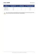
External input voltage
Circuit-limiting resistance Rlimit
Line0+ input voltage
9V
680Ω
About 5.5V
12V
1kΩ
About 6V
24V
2kΩ
About 10V
Table 7-3 Circuit-limiting resistor value
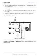
The connection method of the opto-isolated input circuit and the NPN and PNP photosensor is shown in
Figure 7-2 and Figure 7-3. The relationship between the pull-up resistor and the external power supply
voltage is shown in Table 7-3.
3.3V
Line0+
Line0-
FPGA INPUT0
External circuit
Camera internal circuit
Signal output
Power +
PWR GND
NPN
Pull-up
resistor
9
1
2
3
4
5
6
7
8
12
11
10
Figure 7-2 NPN photosensor connected to opto-isolated input circuit
3.3V
Line0
+
Line0-
FPGA INPUT0
External circuit
Camera internal circuit
Signal output
Power +
PWR GND
PNP
9
1
2
3
4
5
6
7
8
12
11
10
Current limiting
resistor
Figure 7-3 PNP photosensor connected to opto-isolated input circuit
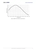
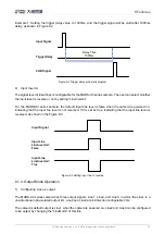
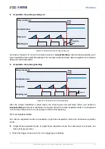
Rising edge delay: <50μs (0°C~45°C), parameter description as shown in
Falling edge delay
: <50μs (0°C~45°C), parameter description as shown in
Different environment temperature and input voltage have influence on delay time of opto-isolated input
circuit. Delay times in typical application environment (temperature is 25°C) is as shown in


