2
SAFETY&PRECAUTIONS
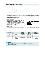
SAFETY CHECK AFTER SERVING
Examine the area surrounding the repaired location for damage or deterioration. Observe that screw, parts and wires
have been returned to original positions. Afterwards, perform the following tests and conform the specified values in order
to verify compliance whit safety standards.
1. Insulation resistance test
Confirm the specified insulation resistance between power cord plug prong and externally exposed parts of the set
(RF terminals, antenna terminals, video and audio input and output terminals, microphone jacks, earphone jacks, etc.)
isgreater than values given in table 1 below.
2. Dielectric strengthen test
Confirm specified dielectric strengthen between power cord
plug prongs and exposed accessible parts of the set
(RF terminals, antenna terminals, video and audio input output
terminals, microphone jack, ear phone jacks, etc.)
is greater than values given table 1.
3. Clearance distance
When replacing primary circuit component, confirm specified clearance distance (d), (d
’
) between soldered terminals,
and between terminals and surrounding metallic parts. See table below.
Rating for selected areas
* : Class model only
AC Line Voltage
Region
Insulation
Resistance
Dielectric
Strength
Clearance
Distance(d),(d)
100V
Japan
>
1
M
Ω
/500V DC
1kV
AC 1min.
>
3
110 to 130V
USA & Canada
-
900V AC 1min.
>
3.2
* 110 to 130V
200 to 240V
Europe
Australia
Latin America
>
10
M
Ω
/500V DC
4kV AC 1min.
>
6(d)
>
8(d')
(a :Power cord)
This table is unofficial and for reference only. Be sure to confirm the precise values for your
particular country and locality
NOTE
Summary of Contents for DV-T1B
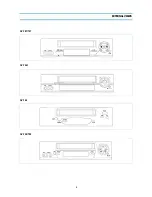
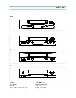
Page 5: ...4 1 FRONT VIEWS FUNCTION DV T8D T5D T 5 DV T87 T57 DV T6A1 DV T8W T5W EXTERNAL VIEWS...
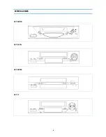
Page 6: ...5 DV T8T T5T DV T5M DV T56 DV T59 T89 EXTERNAL VIEWS...
Page 7: ...6 DV T5B T1B DV T8L T5L DV T8E T5E DV T1T EXTERNAL VIEWS...
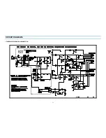
Page 15: ...14 1 POWER SUPPLY SCHEMATIC DIAGRAM VCR S A CIRCUIT DIAGRAM...
Page 16: ...15 2 SERVO SYSCON SCHEMATIC DIAGRAM VCR S A CIRCUIT DIAGRAM...
Page 17: ...16 3 VIDEO AUDIO SCHEMATIC DIAGRAM HIFI CIRCUIT DIAGRAM...
Page 18: ...17 4 VIDEO AUDIO SCHEMATIC DIAGRAM MONO CIRCUIT DIAGRAM...
Page 19: ...18 CIRCUIT DIAGRAM 5 TMI MPX SCHEMATIC DIAGRAM HIFI...
Page 20: ...19 CIRCUIT DIAGRAM 6 TMI MPX SCHEMATIC DIAGRAM MONO...
Page 23: ...22 COMPONENTS LOCATION GUIDE ON PCB BOTTOM VIEW 1 PCB MAIN...
Page 27: ...26 DISASSEMBLY 1 PACKING ASS Y...
Page 43: ......


