


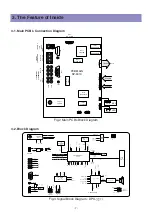


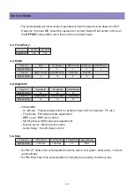

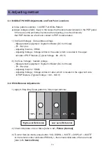
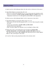


3. The Feature of Inside
-7-
Fig.2 Main PCBs Block Diagram
KEY
LED
PA101
P702
J151
J301
J855
PC851
IC101
PW338B
IC201
DDR SDRAM
IC202
DDR SDRAM
IC401
FLASH 16M
PCB MAIN
SP-901X
AV3
(Y/C, CVBS)
J853
J851
J802
J801
P801
J854
Upgrade
jack
PC
(D-SUB)
DVI & PC
Audio L/R
HDMI
SPDIF
_OUT
S-VIDEO1
MONIT
OR_OUT
VIDEO1
COMPONENT2
COMPONENT1
P701
TU901
TUNER
PA103
IC751
MSP4650K
From PWR
From PWR
TO PDP MODULE
IC622
PIC16F690
IC701
STA515W
PC602
P109
P108
PC301
PC601
3-1. Main PCB’s Connection Diagram
Fig.3 Signal Block Diagram : DPX-
3-2. Block Diagram
Summary of Contents for DPX-32F1BMB
Page 2: ......
Page 8: ...8 The Feature of Inside 3 3 Power Specification...
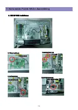
Page 16: ...7 Noticeable Points While Assembling 16...
Page 17: ...Noticeable Points While Assembling 17...
Page 21: ...21 5 Importing HEX file for upgrade Software Upgrade Methord...
Page 37: ...37 Trouble shooting 9 6 No Key and Remote Control Operation...
Page 41: ......
Page 42: ...42 11 Exploded View...