background image

- 51 -

Service manual WP 895/895F, CP885/885F, CP485F

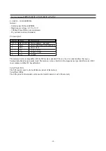
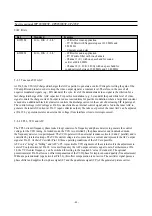
configuration

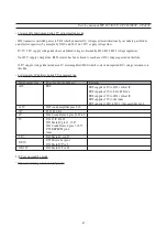
Stand by

TV ON

1

Power

Push Pull Low

Push Pull High

Switch OFF / ON SMPS

2

AGC

High impedance

High impedance

Tuner AGC level input –
For factory use only

5

Mod SW

High impedance

Push Pull

High = Negative
modulation, Low = Positive
modulation (L/L’).

6

SECAM L’

High impedance

Push Pull

Low = L, High =L’

7

AFC

High impedance

High impedance

ADC input

8

IR

High impedance

High impedance

Interrupt input

9

SC1 SW

High impedance

High impedance

SCART 1 slow switching –
ADC input

10

SC2 SW

High impedance

High impedance

SCART 2 slow switching –
ADC input

61

Mute

Push Pull

Push Pull

High = Mute active

62

LED

Open Drain

Open Drain

63

KB

High impedance

High impedance

Keyboard input – ADC
input

64

OCP

High impedance

High impedance

Over Current Protection –
Switch the set to Std by if < 2.

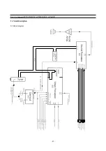
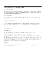
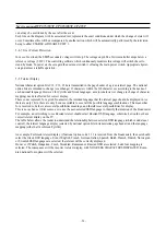
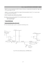
5-4-3   - Controller I/O pin configuration and function

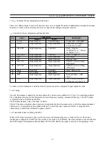
There exist different kinds of ports. The universal ports serve as digital I/O and have additional special input and output
functions. A subset of the universal ports serves as input for the analogue-to-digital converter.

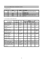
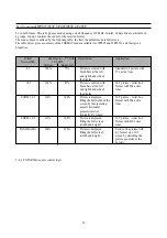
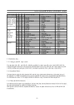
   - Controller I/O pin configuration and function table

pin

name

description

To reduce power consumption in stand by mode all ports not used are configured in high impedance mode.

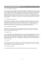
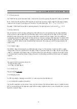
5-4-4  Tuning

The AFC information is supplied by the demodulator IC, and becomes available on VCT pin 7 for controlling software.
The controlling software uses this information for tuner frequency tracking ( automatic following ). The AFC window
is typically between 50 KHz and 100 KHz.
The minimum frequency step of the tuner is 50 Khz.
This AFC function is disabled when a program is tuned using the direct frequency entry or after fine tuning adjustment.
Therefore it is recommended to tune channel with the TV search function ( manual or ATSS ) or using the direct
channel entry to enable the Automatic Frequency Control.

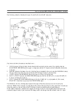
5-4-5 Automatic Format switching and WSS

When AUTO mode is selected by the user, the television will automatically select a mode for the user. The format
information is supplied by SCART pin 8 level when in AV mode or by WSS data. The signal contains codes as defined in
the WSS European Telecommunication Standard, ETS 300 294. Briefly, the signal is received at the beginning of line

Summary of Contents for CP-485F

Page 1: ...levision CHASSIS WP 895 WP 895F CP 885 CP 885F CP 485F Caution In this Manual some parts can be changed for improving their performance without notice in the parts list So if you need the latest parts information please refer to PPL Parts Price List in Service Information Center http svc dwe co kr ...

Page 2: ...ith embedded 8 bit Controller 19 4 1 1 Block diagram off the VCT 19 4 1 2 TV signal Processor 19 4 1 2 Controller 20 4 1 4 Teletext Features 20 4 1 5 Displaty OSD Features 21 4 1 6 Audio Features 21 4 1 7 General Features 21 4 1 8 Data Capture 21 4 1 9 Data Capture Features 21 4 1 10 TV processor version and Controller capacity 22 4 1 11 IC marking and version 22 4 1 12 Pinning 22 4 2 MSP341x Mult...

Page 3: ...rnal Voltage Stabiliser 45 5 3 Video VCT description 46 5 3 1 Introduction 46 5 3 2 Video Front end 46 5 3 3 Input Selector 46 5 3 4 Clamping 46 5 3 5 Automatic Gain Control 46 5 3 6 Digitally Controlled Clock Oscillator 46 5 3 7 Analogue Video Output 46 5 3 8 Adaptive Comb Filter VCT3834A only 47 5 3 9 Color Decoder 47 5 3 10 Horizontal Scaler 47 5 3 11 Video Sync Processing 48 5 3 12 Display Pro...

Page 4: ... 8 1 Flybac k voltage 57 5 8 2 Protection 57 5 8 3 Guard circuit 57 5 8 4 Damping resistor 57 5 8 5 EAST WEST Amplifier TD A8358J only 57 5 9 P ower supply STR F6653 58 5 9 1 STR F6654 gener aral descr iption 58 5 9 2 Power supply primary part operations 58 5 10TV start up TV normal run and stand by mode operations 62 5 10 1 TV start up operations 62 5 10 2 TV normal run and stand by mode operatio...

Page 5: ...Aerial input 75 ohm unbalanced Channel coverage Off air channels S cable channels and hyperband Tuning system frequency synthesiser tuning system Visual screen 21 51 cm 28 66 cm 29 68 cm Channel indication On Screen Display Program Selection 100 programmes Aux terminal EURO SCART 1 Audio Video In and Out R G B In Slow and Fast switching EURO SCART 2 Audio Video In and Out SVHS In AV3 Audio Video J...

Page 6: ... SOUND EFFECTS OFF SPATIAL OFF SPATIAL PANORAMA VIRTUAL DOLBY OFF SPATIAL OFF SPATIAL PANORAMA VIRTUAL DOLBY OFF SPATIAL OFF SPATIAL OFF SPATIAL OFF SPATIAL PANORAMA VIRTUAL DOLBY GRAPHIC EQUALIZER AV3 AUDIO INPUT DEDICATED DEDICATED DEDICATED DEDICATED DEDICATED AV2 COMMON DEDICATED DEDICATED TELETEXT PAGE MEMORY 10 PAGE 10 PAGE 10 PAGE 10 PAGE TOP TELETEXT AVAILABLE SELECTABLE IN FACTORY SERVICE...

Page 7: ... Input 0 7 Vpp 0 1V Impedance 75 16 Fast Switching 0 to 0 4V Logic 0 1 to 3V Logic 1 Impedance 75 17 Video Out Earth 18 Video In Earth 19 Video Output 1 Vpp 3dB Impedance 75 20 Video Input 1 Vpp 3dB Impedance 75 21 Common Earth 21 Pin EURO SCART 2 Pin Signal Description Matching value 1 Audio Output Right 0 5 Vrms Impedance 1 RF 54 Mod Not available for cp885 2 Audio Input Right 0 5 Vrms Impedance...

Page 8: ... 7 Service manual WP 895 895F CP885 885F CP485F 19 Video Output 1 Vpp 3dB Impedance 75 Monitor output Not available for cp885 20 Video Input Y In 1 Vpp 3dB Impedance 75 21 Common Earth ...

Page 9: ...183 75 77 75 C18 192 25 85 75 C19 201 25 C20 C21 471 25 471 25 471 25 471 25 C22 479 25 479 25 479 25 479 25 C23 487 25 487 25 487 25 487 25 C24 495 25 495 25 495 25 495 25 C25 503 25 503 25 503 25 503 25 C26 511 25 511 25 511 25 511 25 C27 519 25 519 25 519 25 519 25 C28 527 25 527 25 527 25 527 25 C29 535 25 535 25 535 25 535 25 C30 543 25 543 25 543 25 543 25 C31 551 25 551 25 551 25 551 25 C32...

Page 10: ...5 759 25 759 25 C58 767 25 767 25 767 25 767 25 C59 775 25 775 25 775 25 775 25 C60 783 25 783 25 783 25 783 25 C61 791 25 791 25 791 25 791 25 C62 799 25 799 25 799 25 799 25 C63 807 25 807 25 807 25 807 25 C64 815 25 815 25 815 25 815 25 C65 823 25 823 25 823 25 823 25 C66 831 25 831 25 831 25 831 25 C67 839 25 839 25 839 25 839 25 C68 847 25 847 25 847 25 847 25 C69 855 25 855 25 855 25 855 25 ...

Page 11: ...2 311 25 311 25 311 25 311 25 S23 319 25 319 25 319 25 319 25 S24 327 25 327 25 327 25 327 25 S25 335 25 335 25 335 25 335 25 S26 343 25 343 25 343 25 343 25 S27 351 25 351 25 351 25 351 25 S28 359 25 359 25 359 25 359 25 S29 367 25 367 25 367 25 367 25 S30 375 25 375 25 375 25 375 25 S31 383 25 383 25 383 25 383 25 S32 391 25 391 25 391 25 391 25 S33 399 25 399 25 399 25 399 25 S34 407 25 407 25 ...

Page 12: ...he pro grams from the selected country and named by the TV controlling softw are Within this group the sorting order is fixed by the A TSS list Group II It contains all the pro grams with a strong signal strength which are not listed in group I Group III It contains all the pro grams with a weak signal strength which are not listed in group I Group IV If two or more programs with the same code are...

Page 13: ...ative video modulation and then a second time with France system selected positive video modulation Special case GB Note for sa tellite recei ver users Before starting ATSS tur n On your satellite r ecei ver and tune SKY NEWS If GB is selected the TV controlling software seeks for programs only in UHF C21 to C70 The sorting order is 1 BBC1 2 BBC2 3 ITV 4 CH4 5 CH5 6 NEWS If two or more identical p...

Page 14: ... high voltage equipment 2 Discharge the high potential of the picture tube before handling the tube The picture tube is highly evacuated and if broken glass fragments will be violently expelled 2 If any Fuse in this TV receiver is blown replace it with the FUSE specified in the Replacement Parts List 3 When replacing a high wattage resistor metal oxide film resistor in the circuit board keep the r...

Page 15: ... exit SERVICE menu press menu key or Std By key 3 2 Service mode navigation Pr Up Down remote keys cycle through the service items available Vol remote keys Decrement Increment the values within range 0 7 digit keys Toggle bits 0 7 in option byte Order Item Default settingh for wp 895 1 PARABOLA 140 2 HOR WIDTH 1100 3 CORNER 80 4 HOR PARAL 1 5 V LINEAR 2 6 EW TRAPEZ 12 7 S CORRECT 15 8 H BOW 100 9...

Page 16: ...TOP text off FASTEXT FLOF off TUBE 4 3 AUTO 4 3 switch to PANORAMA SVHS3 disable 0 TOP text on FASTEXT FLOF on TUBE 16 9 AUTO 4 3 switch to 4 3 X SVHS3 enable Tuner options 00 Philips 01 ALPS 10 Philips AGC intern 11 Daewoo OPTION2 B7 B6 B5 B4 B3 B2 B1 B0 1 Normal I brightness 0 Y Y Y Y Normal I brightness 5 steps See table below OPTION2 bits B2 B1 B0 OPTION2 bits B2 B1 B0 Beam Current mA B2 B1 B0...

Page 17: ...ng and delivery Verification On pushing the shipping AGC key a four digit hexadecimal number is displayed in addition to SHIPPING This number is there to verify the option bits setting that has been entered For example the binary code 0000 0111 OPTION2 1100 0010 OPTION will give 07 C2 hex The order of display is therefore OPTION2 then OPTION when reading from left to right Bit B7 B6 B5 B4 B3 B2 B1...

Page 18: ...CEN Horizontal center to have the picture in the center of the screen 3 4 7 Eau West comection Adjust the PARABOLA HOR WIDTH CORNER HOR PARAL EW TRAPEZ H BOW to compensate for geometrical distorrin Service manual WP 895 895F CP885 885F CP485F 17 For HOR WIDTH adjust for 91 overscan ...

Page 19: ...895 895F CP885 885F CP485F CORNER EW TRAPEZ 3 4 8 AGC Adjust the antenna signal level at 70 dB V 2 Tune a colour bar pattern Find the AGC item in service mode Adjust AGC volume RB10 to bring the cursor to central position 32 ...

Page 20: ...ecoder with embedded 8 bit Controller 4 1 1 Block diagram of the VCT 4 1 2 TV signal Processor Four composite video inputs two S VHS inputs AnalogueYC r C b input Composite video monitor Multistandard colour decoder 1 crystal Multistandard sync decoder Black line detector Adaptive 2H comb filter Y C separator ...

Page 21: ...able timers capture compare module watchdog timer 14 bit PWM for voltage synthesis Four 8 bit PWMs 10 bit ADC with 15 1 input MUX I2C bus master interface 24 programmable I O ports 80C51 controller core standard instruction set and timing 1 s machine cycle 32 128Kx8 bit late programmed ROM 3 12Kx8 bit Auxiliary RAM shared with Display and Acquisition Interrupt controller for individual enable disa...

Page 22: ...Video and Blanking Signal CVBS and from this extracts the required data which is then decoded and stored in memory The extraction of the data is performed in the digital domain The first stage is to select and convert the analogue CVBS signal into a digital form This is done using 8 bit ADC sampling at 20 25 Mhz The digital data services transmitted in the VBI are selected and acquired separately ...

Page 23: ...ilter Panorama Scaler 4 1 11 IC marking and version Chassis OSD languages ATSS countries Text CP885 VCT3832A CP885F VCT3834A WP895F CP485F VCT3834A WP895 VCT3834A Pan European Latin Cyrillic Greek GB France Germany Italy Belgium Spain Austria Poland Switzerland Denmark Finland Netherlands Norway Sweden Ireland Hungary Czech Republic Others 4 1 12 Pinning PSDIP 64 pin 1 Power OUT High SMPS ON Low S...

Page 24: ...lVertical Sawtooth Output 36 EW OUT Vertical Parabola Output 37 SENSE IN SenseADC Input 38 GNDM SUPPLY Ground MADC Input 39 RSW1 OUT Range Switch1 for MeasurementADC 40 RSW2 OUT Range Switch2 for MeasurementADC 41 SVMOUT OUT ScanVelocity Modulation Output 42 ROUT OUT Analog Red Output 43 GOUT OUT Analog Green Output 44 BOUT OUT Analog Blue Output 45 VSUPAB SUPPLY SupplyVoltage Analog Back end 46 G...

Page 25: ...C GND GND S B 3 3V GND GND GND XREF VRD GND 5V B out G out R out SVM out RSW2 RSW1 GND SENSE EW VERTQ VERT HFLB Power 1 2 3 4 5 7 8 9 10 17 19 20 21 22 23 24 25 26 27 28 29 31 30 32 18 11 12 13 14 15 16 6 AGC S B 5V Gnd MOD SW SECAM L AFC RES IR SC1 SW SC2 SW Vout VRT SGND GND 5V Cb in C in Cr in IF IN SC1 IN SC2 IN RCA VIN TEST H out 3 3 V GND FBLIN Rin Gin Bin VPROT SAFETY VCT 383X ...

Page 26: ...etection for terrestrial TV sound standards Precise bit error rate indication Automatic switching from NICAM to FM AM or vice versa Improved NICAM synchronisation algorithm Improved carrier mute algorithm Improved AM demodulation Reduction of necessary controlling Less external components 4 2 1 Basic Features of the MSP 341x 4 2 1 1 Demodulator and NICAM Decoder Section The MSP 341x is designed to...

Page 27: ...ish Scandinavian Spanish and French TV standards high quality stereo sound is transmitted digitally The systems allow two high quality digital sound channels to be added to the already existing FM AM channel The sound coding follows the format of the so called Near Instantaneous Companding System NICAM 728 Transmission is performed using Differential Quadrature Phase Shift Keying DQPSK Table below...

Page 28: ...M Mono NICAM PAL UK D K 6 5 6 2578125 D K1 FM Stereo SECAM East USSR 6 5 6 7421875 D K2 6 5 5 85 D K NICAM FM Mono NICAM Hungary Architecture of MSP341x Pin connections and short description Pin No Pin Name Type Short description 1 TP Out Test pin 2 NC Not Connected 3 NC Not Connected 4 TP Out Test pin 5 TP Out Test pin 6 ADR_SEL In I2C bus Address select 7 STANDBYQ In Standby Low active 8 NC Not ...

Page 29: ...ted 35 VREF1 Reference ground 1 high voltage part 36 SC1_OUT_R Out Scart output 1 right 37 SC1_OUT_L Out Scart output 1 left 38 NC Not Connected 39 AHVSUP Analog power supply 8 0V 40 CAPL_M Volume capacitor MAIN 41 AHVSS Analog ground 42 AGNDC Analog reference voltage high voltage part 43 NC Not Connected 44 NC Not Connected 45 NC Not Connected 46 NC Not Connected 47 NC Not Connected 48 ASG2 Analo...

Page 30: ...ulation figures Alignment free AFC without external reference circuit polarity of the AFC curve is switchable VIF AGC for negative modulated signals peak sync detection and for positive modulation peak white black level detector Tuner AGC with adjustable take over point Alignment free quasi parallel sound QPS mixer for FM NICAM sound IF signals Intercarrier output signal is gain controlled necessa...

Page 31: ...ion 27 28 Vi SIF2 SIF2 input symmetrical 4 3 4 Block diagram Offset 26 18 20 21 14 VCO l switch VCO Control phase shift FPLL VIF amp Loop filter comp optional 4 9 16 AM det FM det 25 24 17 Cref 23 13 22 19 6 7 8 15 11 10 27 28 3 1 2 SIF 1 CAGC 5 Standard Video det VIF CAGC CBL AGC VIF Tuner AGC AGC SIF Tuner SIF 2 SIF input switch SIF amp Take over point Video AFC AFC switch AFC Supply Standard sw...

Page 32: ...sitive input2 4 4 TDA894xJ Stereo AudioAmplif ier The TDA8944J TDA 8946J is a dual channel audio po wer amplifier with an output power of 2 x 7W 2 X 15W at an 8 load and a 12V supply The circuit contains two Bridges Tied Load BTL amplif iers with an all NPN output stage and standby mute logic The TDA8944J comes in a 17 pin DIL power package 4 4 1 Features Few external components Fixed gain Standby...

Page 33: ... 32 Service manual WP 895 895F CP885 885F CP485F Block diagram TDA8944J ...

Page 34: ...S process that combines Bipolar CMOS and DMOS devices MOS transistors are used in the output stage because of the absence of second breakdown 4 5 1 TDA8357J Features Few external components High efficient fully DC coupled vertical output bridge circuit Short rise and fall time of the vertical flyback switch Guard circuit Temperature thermal protection High EMC because of common mode inputs Pinning...

Page 35: ...ble to sink current from the diode modulator circuit Features Few external components Highly efficient fully DC coupled vertical output bridge circuit Short rise and fall time of the vertical flyback switch Guard circuit Temperature thermal protection High EMC because of common mode inputs East West output stage ...

Page 36: ... 35 Service manual WP 895 895F CP885 885F CP485F ...

Page 37: ...l Features Typical bandwidth of 5 5 MHz for an output signal of 60 Vpp High slew rate of 900V s No external components required Very simple application Single supply voltage of 200V Internal reference voltage of 2 5 V Fixed gain of 50 Black current stabilisation BCS circuit Thermal protection Pin description Pin Symbol Description 1 Vi 1 inverting input 1 2 Vi 2 inverting input 2 3 Vi 3 inverting ...

Page 38: ... 37 Service manual WP 895 895F CP885 885F CP485F Block diagram TDA6107Q ...

Page 39: ...utput 6 SCL Serial clock 7 WC Write control 8 Vcc Supply voltage 4 Vss Ground The memory device is compatible with the I2C memory standard This is a two wire serial interface that uses a bi directionnal data bus and serial clock The memory carries a built in 4 bit unique device type identifier code 1010 in accordance with the I2C bus definition Serial Clock SCL The SCL input is used to strobe all ...

Page 40: ...d in MOSFET and control IC designed for flyback converter type switch mode power supply applications 4 8 2 Features Small SIP fully isolated molded 5 pins package Many protection functions Pulse by pulse overcurrent protection OCP Overvoltage protection with latch mode OVP Thermal protection with latch mode TSD 4 8 3 Block diagram ...

Page 41: ...off 9 10 11 V Circuit current in 4 5 IIN on 30 mA operation Circuit current in non 4 5 IIN off 100 A operation Maximum OFF time TOFF max 45 55 SEC Minimum time for input of 1 5 TTH 2 1 0 SEC quaxi resonant signals Minimum off time TOFF min 1 5 SEC O C P F B terminal 1 5 VTH 1 0 68 0 73 0 78 V threshold voltage 1 O C P F B terminal 1 5 VTH 2 1 3 1 45 1 6 V threshold voltage 2 O C P F B terminal ext...

Page 42: ...4 8 6 MOSFET electrical characteristics IC PINS RATING NUMBER MIN TYPE MAX Drain to source break 3 2 VDSS 650 V voltage Drain leakage current 3 2 IDSS 300 A On resistance 3 2 RDS on 1 15 Switching time 3 2 tf 250 sec Thermal resistance rH F 0 95 0 C W SYMBOL UNIT ...

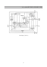
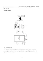
Page 43: ... 42 Service manual WP 895 895F CP885 885F CP485F 5 Circuit description 5 1 Block diagram ...

Page 44: ... the differential input Pin 6 7 of the VIF amplifier 5 2 2 Vision IF Amplifier This amplifier consists of three AC coupled amplifier stages Each differential amplifier is gain controlled by the automatic gain control circuit VIF AGC The output signal of the VIF amplifier is applied to the FPLL carrier generation and the video demodulator ...

Page 45: ...fed to the tuner AGC to generate the tuner AGC current at Pin 11 open collector output The take over point of the tuner AGC can be adjusted at Pin 10 by a potentiometer or an external dc voltage from interface circuit or microprocessor 5 2 4 FPLL VCO and AFC The FPLL circuit frequency phase locked loop consists of a frequency and phase detector to generate the control voltage for the VCO tuning In...

Page 46: ...tion The SIF AGC is related to the average level of AM or FM carrier and controls the SIF amplifier to provide a constant SIF signal to the AM demodulator and QPS mixer 5 2 7 Quasi Parallel Sound QPS Mixer The QPS mixer is realised by a multiplier The SIF signal FM or NICAM carrier is converted to the intercarrier frequency by the regenerated picture carrier quadrature signal which is provided fro...

Page 47: ...of S VHS carrier chrominance signal These inputs are internally biased and have a fixed gain amplifier 5 3 4 Clamping The composite video input signals are AC coupled to the IC The clamping voltage is stored on the coupling capacitors and is generated by digitally controlled current sources The clamping level is the back porch of the video signal S VHS chrominance is also AC coupled The input pin ...

Page 48: ...re for all colour standards The colour killer uses the burst phase burst frequency measurement to identify a PAL NTSC or SECAM colour signal For PAL NTSC the colour is switched off killed as long as the colour subcarrier PLL is not locked For SECAM the killer is controlled by the toggle of the burst frequency The burst amplitude measurement is used to switch off the colour if the burst amplitude i...

Page 49: ...uit TheYC r C b signals are converted by a program mable matrix to RGB colour space The digital OSD insertion circuit allows the insertion of a 5 bit OSD signal The OSD signals and the display clock are synchronised to the horizontal flyback 5 3 13 Chroma Transient Improvement The intention of this block is to enhance the chroma resolution A correction signal is calculated by differentiation of th...

Page 50: ...switch back to BCL limited drives and brightness 5 3 17 Analogue RGB Insertion The VCT 38xxA allows insertion of external analogue RGB signals The RGB signal is key clamped and inserted into the main RGB by the Fast Blank switch The external RGB input can be overlaid or underlaid to the digital picture The external RGB signals can be adjusted independently as regards DC level brightness and magnit...

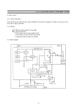
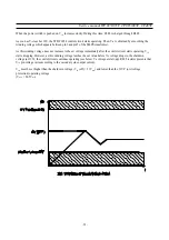
Page 51: ...nd digital circuitry VSUP D 5 4 Microcontroller 5 4 1 Introduction The TV controller basically consists of the CPU RAM ROM and a number of peripheral modules For instance a memory banking module is included to allow access to more than 64 kB memory a bootloader software is included to allow in system downloading of external code to Flash memory via the I 2 C interface The TV controller runs the co...

Page 52: ...l ports serves as input for the analogue to digital converter Controller I O pin configuration and function table pin name description To reduce power consumption in stand by mode all ports not used are configured in high impedance mode 5 4 4 Tuning The AFC information is supplied by the demodulator IC and becomes available on VCT pin 7 for controlling software The controlling software uses this i...

Page 53: ...horizontal geometrical error typically 8 linear ZOOM 16 9 133 100 Picture is displayed 16 9 picture letter box filling the full screen format with 430 active width and height lines PANORAMA 100 100 Picture is displayed Used to fit a picture with filling the full screen 4 3 format on a 16 9 width and height screen by stretching the picture geometry at the borders 23 in each frame This is bi phase e...

Page 54: ...ol or on the television 4 S SW 1 or S SW 2 represent the SLOW SWITCHING inputs of the first SCART AV 1 or second SCART AV 2 these each being pin number 8 5 F SW 1 represents the FAST SWITCHING input of the first SCART AV 1 on pin number 16 The second SCART AV 2 input does not possess a FAST SWITCHING input The HIGH state of a slow switching input represents the request from the external source to ...

Page 55: ...ent for a given broadcaster the intended language that the teletext page should be displayed in As there are only 3 bits there are only 8 codes available to cover all the possible language combinations This means that for a received code there are several possibilities meanings and therefore several possibilities for display This is not as bad as it first seems as we use the user selected OSD lang...

Page 56: ...German Italian Spanish Dutch Danish Finnish Norwegian Swedish Greek Polish Hungarian Czech Slovakian Rumanial Russian 5 6 Sound processing 5 6 1 Analogue sound IF input section The input pins ANA_IN1 and ANA_IN offer the possibility to connect sound IF sources to the MSP 341xD The analogue to digital conversion of the preselected sound IF signal is done by an A D converter whose output is used to ...

Page 57: ... the signal quality and automatically switches to the analogue sound carrier 1 if the transmission quality is too poor To avoid unwanted automatic switching the threshold levels mono to stereo and stereo to mono are different In forced mono mode Red OSD in status Display Window the controlling software configures the MSP341xD to demodula te onl y the analogue FM or AM sound carrier 1 no matter the...

Page 58: ...tput current through the deflection coils measured as voltage across R398 which provides internal feedback information The voltage across R398 is proportional to the output current 5 8 1 Flyback voltage The flyback voltage is determined by an additional supply voltage Vflb The principle of operation with two supply voltages class G makes it possible to fix the supply voltage Vp optimum for the sca...

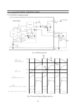
Page 59: ...d control IC designed for flyback converter type switch mode power supply applications 5 9 2 Power supply primary part operations An oscillator generates pulses signals which turn on and off a MOSFET transistor 5 9 2 1 Start up circuit VIN The start up circuit is used to start and stop the operation of the control IC by detecting a voltage appearing at VIN pin pin 4 ...

Page 60: ...nding voltage does not increase to the set voltage immediately after the control circuit starts operating VIN starts dropping However as this winding voltage reaches the set value before VIN voltage drops to the shutdown voltage at 11V the control circuit continues operating see below VIN voltage at start up R805 resistor prevents that VIN pin voltage varies according to the secondary side output ...

Page 61: ... 60 Service manual WP 895 895F CP885 885F CP485F 5 9 2 2 STR F6654 oscillating operation ...

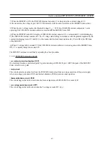
Page 62: ...time determined by C1 and R1 is the OFF time of the MOSFET When C1 voltage falls to around 3 7V the STR F6654 internal oscillator is reversed again and the MOSFET turns ON C1 is quickly charged to around 6 5V The MOSFET continues to oscillate by repeating the above procedure 5 9 2 3 STR F6654 protection circuits overcurrent protection function OCP Overcurrent protection is performed pulse by pulse...

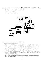
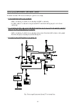
Page 63: ...r and There regulators provide 5V 3 3V DC voltage to I501 microcontroller power supply pins pin 3 pin 54 and to the reset pulse circuit which provides reset pulse to I501 microcontroller reset pin pin 58 Then the microcontroller starts its initialisation Its power pin pin 1 is set to high which allows delivery of power supply voltages 123V 143V 8V 5V At this step all IC s start working but no pict...

Page 64: ... before switching off the microcontroller switches TV set to stand by mode decreasing power pin voltage pin 1 5 10 2 TV normal run and stand by mode operations Depending on remote control commands I501 microcontroller part pin 1 power is set to high for normal run mode low for stand by mode a TV on normal run mode I501 microcontroller part pin 1 power effect I501 microcontroller part pin 1 power i...

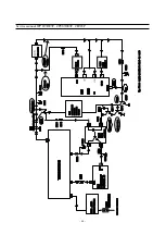
Page 65: ...onnected to the ground and I810 controlled rectifier gate pin is set to low no conducting So current from 14V DC voltage from T801 SMPS transformer pin 13 does not flow through Q811 and Q810 transistors but flows through I806 IC error amplifier Q809 is conducting So Q810 is not conducting and no current flows from Q810 collector to the ground Therefore the power circuit diagram is the following on...

Page 66: ... an IC error amplifier I806 which corrects unexpected DC voltage variations on this line power supply IC delivery during TV set normal run power supply line IC power supply delivery Remarks 143V FBT FBT supplies 43V to I301 vertical IC FBT supplies 43V to T401 H Drive FBT supplies 12V to I301 vertical IC FBT supplies 33V to the tuner FBT supplies 188V to I901 video amplifier pin 6 14 5V I602 sound...

Page 67: ... 66 Service manual WP 895 895F CP885 885F CP485F ...

Page 68: ...trolled rectifier gate pin is set to high and I810 is conducting So current flows from pin 16 SMPS transformer to the ground via I804 optocoupler and Q810 and Q811 transistors which are conducting In these conditions I801 delivers pulses on light mode and T801 produces voltages with reduced power As I810 is conducting current flows also from pin 16 SMPS transformer to I823 5V 3 3V regulator for I5...

Page 69: ...00 BAG P E PE FOAM t0 5x1600x1270 0000A 4857027800 HEAT SINK AL EX 0000B 7174300811 SCREW TAPPTITE TT2 RND 3X8 MFZN SP01 4858311110 SPEAKER 12W 8 OHM SP 58126F SP02 4858311110 SPEAKER 12W 8 OHM SP 58126F PW001 4857417700 TERM CLAMP PT 01 T3 ZZ290 PTMPMSX28W5ZF PCB MAIN MANUAL AS DWX 28W5ZZF 10 2193100801 SOLDER BAR SN PB 63 37 3PI NO FLUX 40 2291050314 FLUX SOLVENT IM 1000 20 2193011101 SOLDER WIR...

Page 70: ...0 CONN WAFER YPW500 02 Q401 T2SD1880 TR 2SD1880 Q401A 4857024500 HEAT SINK AL EX Q401B 7174300811 SCREW TAPPTITE TT2 RND 3X8 MFZN R398 RD 2Z109J R CARBON FILM 1 2 1 OHM J R399 RS02Y180JS R M OXIDE FILM 2W 18 OHM J SMALL R415 RS02Y102JS R M OXIDE FILM 2W 1K OHM J SMALL R450 RS02Y223JS R M OXIDE FILM 2W 22K OHM J SMALL R801 DPC7R0M290 POSISTOR 96709 PHILIPS R802 RS02Y753JS R M OXIDE FILM 2W 75K OHM ...

Page 71: ...0V RSS 1MF 5X11 TP C614 CEXF1H109V C ELECTRO 50V RSS 1MF 5X11 TP C615 CEXF1H109V C ELECTRO 50V RSS 1MF 5X11 TP C616 CEXF1H100V C ELECTRO 50V RSS 10MF 5X11 TP C617 CBXF1H104Z C CERA SEMI 50V F 0 1MF Z TAPPING C622 CXCH1H680J C CERA 50V CH 68PF J TAPPING C623 CEXF1H109V C ELECTRO 50V RSS 1MF 5X11 TP C624 CEXF1H109V C ELECTRO 50V RSS 1MF 5X11 TP C625 CEXF1E101V C ELECTRO 25V RSS 100MF 6 3X11 TP C626 ...

Page 72: ...1H220J C CERA 50V SL 22PF J AXIAL C163 CCZF1H103Z C CERA 50V F 0 01MF Z C500 CCZF1H103Z C CERA 50V F 0 01MF Z C501 CCZF1H103Z C CERA 50V F 0 01MF Z C503 CBZF1H104Z C CERA SEMI 50V F 0 1MF Z AXIAL C505 CCZB1H102K C CERA 50V B 1000PF K AXIAL C506 CBZF1H104Z C CERA SEMI 50V F 0 1MF Z AXIAL C507 CCZF1H103Z C CERA 50V F 0 01MF Z C509 CCZF1H103Z C CERA 50V F 0 01MF Z C512 CCZF1H103Z C CERA 50V F 0 01MF ...

Page 73: ...2 DBAV21 DIODE BAV21 TAPPING D913 DBAV21 DIODE BAV21 TAPPING D997 DBYT51J DIODE BYT51J TAPPING DA10 DTZX5V6B DIODE ZENER TZX5V6B TAPPING DA11 DTZX5V6B DIODE ZENER TZX5V6B TAPPING DA15 DTZX5V6B DIODE ZENER TZX5V6B TAPPING DA16 DTZX5V6B DIODE ZENER TZX5V6B TAPPING DA20 DTZX5V6B DIODE ZENER TZX5V6B TAPPING DA27 DTZX5V6B DIODE ZENER TZX5V6B TAPPING DA3 DTZX5V1B DIODE ZENER TZX5V1B TAPPING DA32 DTZX5V6...

Page 74: ...OPPER AWG22 1 0 65 TIN COATING J883 85801065GY WIRE COPPER AWG22 1 0 65 TIN COATING J885 85801065GY WIRE COPPER AWG22 1 0 65 TIN COATING J887 85801065GY WIRE COPPER AWG22 1 0 65 TIN COATING J888 85801065GY WIRE COPPER AWG22 1 0 65 TIN COATING J889 85801065GY WIRE COPPER AWG22 1 0 65 TIN COATING J891 85801065GY WIRE COPPER AWG22 1 0 65 TIN COATING J896 85801065GY WIRE COPPER AWG22 1 0 65 TIN COATIN...

Page 75: ... 10K OHM J R532 RD AZ223J R CARBON FILM 1 6 22K OHM J R533 RD AZ103J R CARBON FILM 1 6 10K OHM J R535 RD AZ201J R CARBON FILM 1 6 200 OHM J R537 RD AZ201J R CARBON FILM 1 6 200 OHM J R540 RD AZ101J R CARBON FILM 1 6 100 OHM J R541 RD AZ122J R CARBON FILM 1 6 1 2K OHM J R542 RD AZ223J R CARBON FILM 1 6 22K OHM J R543 RD AZ271J R CARBON FILM 1 6 270 OHM J R544 RD AZ222J R CARBON FILM 1 6 2 2K OHM J ...

Page 76: ...OHM J R829 RD AZ103J R CARBON FILM 1 6 10K OHM J R830 RD AZ332J R CARBON FILM 1 6 3 3K OHM J R841 RD 2Z470J R CARBON FILM 1 2 47 OHM J R851 RD AZ391J R CARBON FILM 1 6 390 OHM J R852 RD AZ102J R CARBON FILM 1 6 1K OHM J R855 RD 4Z335J R CARBON FILM 1 4 3 3M OHM J R870 RD 2Z222J R CARBON FILM 1 2 2 2K OHM J R901 RD AZ221J R CARBON FILM 1 6 220 OHM J R902 RD AZ221J R CARBON FILM 1 6 220 OHM J R903 R...

Page 77: ...TRO 400V LHS 180MF 25X35 C811 CCYR3D681K C CERA 2KV R 680PF K 125C C812 CH1AFE472M C CERA AC 4KV 4700PF M KX DE1610 C813 CEXF2E101V C ELECTRO 250V RSS 100MF 18X35 5 C814 CEYF2E470V C ELECTRO 250V RSS 47MF 16X25 C820 CCYR3A471K C CERA 1KV 470PF K 125C C823 CEXF1E102V C ELECTRO 25V RSS 1000MF 13X20 TP C832 CEXF1E102V C ELECTRO 25V RSS 1000MF 13X20 TP C840 CEXF1C222V C ELECTRO 16V RSS 2200MF 13X25 TP...

Page 78: ...IPTION REMARK C508 CEXF1H220V C ELECTRO 50V RSS 22MF 5X11 TP C510 CCXF1H473Z C CERA 50V F 0 047MF Z TAPPING C511 CEXF1E100V C ELECTRO 25V RSS 10MF TP C519 CEXF1H109V C ELECTRO 50V RSS 1MF 5X11 TP C520 CEXF1H109V C ELECTRO 50V RSS 1MF 5X11 TP C521 CEXF1H109V C ELECTRO 50V RSS 1MF 5X11 TP C522 CEXF1H109V C ELECTRO 50V RSS 1MF 5X11 TP C525 CEXF1H220V C ELECTRO 50V RSS 22MF 5X11 TP C528 CCXF1H223Z C C...

Page 79: ...1K C CERA 50V B 470PF K AXIAL CA16 CCZB1H471K C CERA 50V B 470PF K AXIAL CA17 CCZB1H471K C CERA 50V B 470PF K AXIAL LOC PART CODE PART NAME DESCRIPTION REMARK CA18 CCZB1H471K C CERA 50V B 470PF K AXIAL CA19 CCZB1H222K C CERA 50V B 2200PF K AXIAL CA2 CCZB1H101K C CERA 50V B 100PF K AXIAL CA20 CCZB1H222K C CERA 50V B 2200PF K AXIAL CA3 CCZB1H101K C CERA 50V B 100PF K AXIAL CA4 CCZB1H102K C CERA 50V ...

Page 80: ...AWG22 1 0 65 TIN COATING J921 85801065GY WIRE COPPER AWG22 1 0 65 TIN COATING J924 85801065GY WIRE COPPER AWG22 1 0 65 TIN COATING J925 85801065GY WIRE COPPER AWG22 1 0 65 TIN COATING J926 85801065GY WIRE COPPER AWG22 1 0 65 TIN COATING L105 5CPZ479K02 COIL PEAKING 4 7UH 3 5MM K LAL02TB L153 5CPZ120K02 COIL PEAKING 12UH 3 5MM K LAL02TB L501 5CPZ479K02 COIL PEAKING 4 7UH 3 5MM K LAL02TB LOC PART CO...

Page 81: ...RBON FILM 1 6 1K OHM J R710 RD AZ102J R CARBON FILM 1 6 1K OHM J LOC PART CODE PART NAME DESCRIPTION REMARK R711 RD AZ103J R CARBON FILM 1 6 10K OHM J R712 RD AZ181J R CARBON FILM 1 6 180 OHM J R713 RD AZ331J R CARBON FILM 1 6 330 OHM J R720 RD AZ122J R CARBON FILM 1 6 1 2K OHM J R721 RD AZ181J R CARBON FILM 1 6 180 OHM J R722 RD AZ221J R CARBON FILM 1 6 220 OHM J R723 RD AZ331J R CARBON FILM 1 6 ...

Page 82: ... TP C866 CCYR3A471K C CERA 1KV 470PF K 125C C900 CCXB3D102K C CERA 2KV B 1000 PF K TAPPING C910 CEXF2E479V C ELECTRO 250V RSS 4 7MF 10X16 TP C997 CEXF2E100V C ELECTRO 250V RSS 10MF 10X20 TP D403 DDG3 DIODE DG3 D820 DRGP30J DIODE RGP30J D860 DRGP30J DIODE RGP30J F801 5FSCB4022R FUSE CERA SEMKO F4AH 4A 250V MF51 G900 4SG0DX0001 SPARK GAP SSG 102 A1 1 0KV I101 1TDA4470M IC IF TDA4470 M I301 1TDA8358J...

Page 83: ...X11 TP C608 CEXF1E100V C ELECTRO 25V RSS 10MF TP C610 CEXF1E100V C ELECTRO 25V RSS 10MF TP C611 CEXF1H339V C ELECTRO 50V RSS 3 3MF 5X11 TP C612 CEXF1H109V C ELECTRO 50V RSS 1MF 5X11 TP LOC PART CODE PART NAME DESCRIPTION REMARK C613 CEXF1H109V C ELECTRO 50V RSS 1MF 5X11 TP C614 CEXF1H109V C ELECTRO 50V RSS 1MF 5X11 TP C615 CEXF1H109V C ELECTRO 50V RSS 1MF 5X11 TP C616 CEXF1E100V C ELECTRO 25V RSS ...

Page 84: ...RIPTION REMARK D521 D1N4148 DIODE 1N4148 TAPPING D533 D1N4148 DIODE 1N4148 TAPPING D534 D1N4148 DIODE 1N4148 TAPPING D537 D1N4148 DIODE 1N4148 TAPPING D550 D1N4148 DIODE 1N4148 TAPPING D551 D1N4148 DIODE 1N4148 TAPPING D591 DUZ2R7B DIODE ZENER UZ 2 7B D597 D1N4148 DIODE 1N4148 TAPPING D598 D1N4148 DIODE 1N4148 TAPPING D599 DTZX5V6B DIODE ZENER TZX5V6B TAPPING D601 D1N4148 DIODE 1N4148 TAPPING D602...

Page 85: ...ARBON FILM 1 6 2 2K OHM J R116 RD AZ682J R CARBON FILM 1 6 6 8K OHM J R117 RD AZ682J R CARBON FILM 1 6 6 8K OHM J R118 RD AZ151J R CARBON FILM 1 6 150 OHM J R120 RD AZ101J R CARBON FILM 1 6 100 OHM J R131 RD AZ472J R CARBON FILM 1 6 4 7K OHM J R151 RD AZ102J R CARBON FILM 1 6 1K OHM J R152 RD AZ271J R CARBON FILM 1 6 270 OHM J LOC PART CODE PART NAME DESCRIPTION REMARK R153 RD AZ470J R CARBON FILM...

Page 86: ... 1 4 1K OHM J R823 RD 4Z682J R CARBON FILM 1 4 6 8K OHM J LOC PART CODE PART NAME DESCRIPTION REMARK R829 RD AZ103J R CARBON FILM 1 6 10K OHM J R830 RD AZ332J R CARBON FILM 1 6 3 3K OHM J R841 RD 2Z470J R CARBON FILM 1 2 47 OHM J R851 RD AZ391J R CARBON FILM 1 6 390 OHM J R852 RD AZ102J R CARBON FILM 1 6 1K OHM J R855 RD 4Z335J R CARBON FILM 1 4 3 3M OHM J R870 RD 2Z222J R CARBON FILM 1 2 2 2K OHM...

Page 87: ...Service Manual WP 895 895F CP885 885F CP485F 86 7 Exploded View 7 1 DWX 28W5 ...

Page 88: ...Service Manual WP 895 895F CP885 885F CP485F 87 7 Exploded View 7 2 DWF 28W8 ...

Page 89: ...Service Manual WP 895 895F CP885 885F CP485F 88 7 Exploded View 7 3 DTF 29U8 ...

Page 90: ...Service Manual WP 895 895F CP885 885F CP485F 89 7 Exploded View 7 4 DTP 28A7 ...

Page 91: ...Service Man ual WP 895 895F CP885 885F CP485F 90 7 Exploded View 7 5 DTP 28B1 ...

Page 92: ...Service Man ual WP 895 895F CP885 885F CP485F 91 7 Exploded View 7 6 DTP 28G7 ...

Page 93: ...Service Manual WP 895 895F CP885 885F CP485F 92 7 Exploded View 7 7 DTP 28G8 ...

Page 94: ...Service Manual WP 895 895F CP885 885F CP485F 7 8 DWF 28W9 93 7 Exploded View ...

Page 95: ... 94 Service Manual WP 895 895F CP885 885F CP 485F 7 9 DTB 21U7 7 Exploded view ...

Page 96: ...SCHEMATIC DIAGRAM WP 895 CP 885 ...

Page 97: ...SCHEMATIC DIAGRAM WP 895F CP 885F ...

Page 98: ...SCHEMATIC DIAGRAM CP 485F ...

Page 99: ......

Page 100: ......

Page 101: ... CP 485F ...

Page 102: ...686 AHYEON DONG MAPO GU SEOUL KOREA C P O BOX 8003 SEOUL KOREA TELEX DWELEC K28177 8 CABLE DAEWOOELEC ...

Reviews: