Service manual CP-785AF
- 37 -
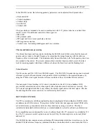
5-6 Sound amplification
The TDA8946J is a stereo BTL audio amplifier capable of delivering 2 x 7 W output power to
an 8
Ω
load at THD = 10%, using a 12 V power supply and an external heatsink. The voltage
gain is fixed at 32dB.
With the three-level MODE input the device can be switched from ‘ standby’ to ‘ mute’ and to
‘ operating’ mode.
The TDA 8946J outputs are protected by an internal thermal shutdown protection mechanism and
short-circuit protection.
Power amplifier
The power amplifier is a Bridge Tied Load (BTL) amplifier with an all-NPN output stage, capable of
delivering a peak output current of 1.5 A.
The BTL principle offers the following advantages :
- Lower peak value of the supply current.
- The ripple frequency on the supply voltage is twice the signal frequency.
- No DC-blocking capacitor
- Good low frequency performance
Mode selection
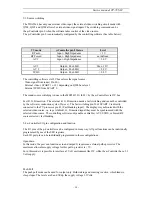
The TDA894xJ has several functional modes, which can be selected by applying the proper DC voltage
to pin MODE.
Mute : In this mode the amplifier is DC biased but not operational (no audio output). This allows the
input coupling capacitors to be charged to avoid pop-noise. The devices is in mute mode when 2.5 V <
V
MODE
< (Vcc-1.5 V).
Operating : In this mode the amplifier is operating normally. The operating mode is activated at V
MODE
< 0.5 V.
5-7 Vertical deflection
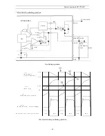
The vertical driver circuit is a bridge configuration. The deflection coil is connected between the output
amplifiers, which are driven in phase opposition. The differential input circuit is voltage driven. The
input circuit is especially intended for direct connection to driver circuits which deliver symmetrical
current signals, but is also suitable for asymmetrical currents. The output current of these devices is
converted to voltages at the input pins via resistors R350 and R351. The differential input voltage is
compared with the output current through the deflection coils measured as voltage across R302, which
provides internal feedback information. The voltage across R302 is proportional to the output current.
Flyback voltage
The flyback voltage is determined by an additional supply voltage V
flb
. The principle of operation with
two supply voltages (class G) makes it possible to fix the supply voltage Vp optimum for the scan
voltage and the second supply voltage V
flb
optimum for the flyback voltage. Using this method, very
high efficiency is achieved. The supply voltage V
flb
is almost totally available as flyback voltage across
the coil, this being possible due to the absence of a coupling capacitor.
Protection
The output circuit has protection circuits for :
- Too high die temperature
- overvoltage of output stage A
Guard circuit
The guard signal is not used by the TDA936x to blank the screen in case of fault condition.
Damping resistor
Summary of Contents for DTE-21U6TH
Page 15: ...Service manual CP 785AF A 14...
Page 18: ...Service manual CP 785AF 17...
Page 30: ...Service manual CP 785AF 29 5 Circuit description 5 1 Block diagram...
Page 60: ...Service manual CP 785AF 59 7 Exploded view...
Page 61: ...Service manual CP 785AF 60 8 PCB Layout...
Page 62: ...S ervice manual CP 785AF 61 9 Circuit Diagram...


