background image

32

TROUBLE SHOOTING

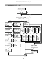
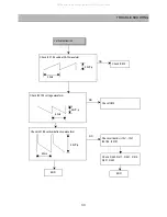
High voltage drive

Check F401 #10 (HVG B+135V)

If resistance between Q430 collector and

base is near, horizontal output TR has

been destroyed.Replace the TR.

Check R445 

Check F401 (High
Voltage Generator)
font

Check F401 #7 (OVP) high voltage
control oscillating waveform

Check R447

Replace I421

No

No

Yes

Q891 Base 0V

Horizontal
Deflection

Check F401 #8 (HVG B+135V)

Voltage waveform of Q430 collector is
shown below.

When power isn’t supplied

END

1000 50Vp-p

NO

NO

END

NO

45VP-p

All manuals and user guides at all-guides.com

Summary of Contents for DSJ-4710CRU

Page 1: ...ist So if you need the latest parts information please refer to PPL Parts Price List in Service Information Center http svc dwe co kr DAEWOO ELECTRONICS Corp Service Manual Aug 2004 S M No DSJ113FEFO...

Page 2: ...agram 1 Block Diagram 51 2 Power 52 3 Convergence Amp 53 4 Convergence Module 54 5 CRT Amp 55 6 IF Module 56 7 AV Main 57 8 Micom Module 58 9 Control Union 59 9 PRINTED CIRCUIT BOARD 1 Main PCB 60 2 P...

Page 3: ...part needs to be replaced Because some electronic parts and appliances have safety related features an electric shock file or X RAY radiation can be caused if no equal rated parts are used 5 When a pa...

Page 4: ...to remove a high voltage cable a Make a discharger to discharge a high voltage b Remove the power cord and wait for 30 sec c Remove the anode cable after discharging as the method mentioned below 2 Ho...

Page 5: ...1 S20 UHF Hyper Band S21 S41 Band IV V CH21 CH69 Screen Size 119cm 47 Signal Method PAL B G I I SECAM B G D K L L Speaker Output 10W ch Main L R Power 220 240V 50 60Hz Power Consumption 195W 1110 x 12...

Page 6: ...tates from Normal News Music Movie Favorite Still Menu Use it to make picture adjustment screen format sound adjustment function install Zoom Off Zoom1 Zoom2 Program OK Childlock Mono Forced Mono Ster...

Page 7: ...t the slant and position of DY so that the rectangle projections of DY are shown in front of the set Figure 1 Front part of CRT assembly Step 2 Fixation of VM coil 1 Tighten the screw completely with...

Page 8: ...it when the line disappears completely 3 Control Red VR Green VR and Blue VR in the order 4 Fix the VR by lock paint after the control is completed Note This control should be performed in a darkroom...

Page 9: ...focus readjustment or correction if the entire screen isn t focused even after the completion of focus control 3 Project R G B signal only by one color using a lens cover and control G R and B in the...

Page 10: ...the horizon of G 5 In the center of screen locate the vertical line of R approx 20 to 30mm to the left on the basis of G and the vertical line of G approx 20 to 30mm to the right Refer to Figure 4 Ste...

Page 11: ...the monitor of control PC the control is completed Measuring unit Multimedia Display Tester 3298 YOKOGAYA Measuring signal White Balance Control Pattern Intra office signal cable broadcasting 32CH Co...

Page 12: ...Screen mode Standard 1 Receive RETMA pattern intra office signal cable broadcasting 96 CH 2 Press the S8 key 3 Control the Sub Brightness so that 18 gradation can be identified in the contrast chart o...

Page 13: ...rt Descriptions for VSPB For VSP 941x 4x the pin connections differ for pins 1 2 3 75 76 77 78 79 80 see Section 5 1 2 on page 210 5 1 1 Common Pin Connections and Short Descriptions VSP94X5B VSP94X7B...

Page 14: ...13 IC Description All manuals and user guides at all guides com...

Page 15: ...14 IC Description All manuals and user guides at all guides com...

Page 16: ...15 IC Description All manuals and user guides at all guides com a l l g u i d e s c o m...

Page 17: ...16 IC Description All manuals and user guides at all guides com...

Page 18: ...17 IC Description 5 1 2 Differing Pin Connections and Short Descriptions for VSP 941xB and VSP 944xB All manuals and user guides at all guides com...

Page 19: ...18 IC Description 5 2 Pin Circuits VSP94X5B VSP94X7B All manuals and user guides at all guides com...

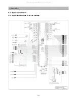
Page 20: ...19 IC Description 5 3 Application Circuit 5 3 1 Application Example for QFP80 package All manuals and user guides at all guides com...

Page 21: ...20 IC Description 5 4 Pin Description CXA2150AQ All manuals and user guides at all guides com a l l g u i d e s c o m...

Page 22: ...21 IC Description All manuals and user guides at all guides com...

Page 23: ...22 IC Description All manuals and user guides at all guides com...

Page 24: ...23 IC Description All manuals and user guides at all guides com...

Page 25: ...24 IC Description All manuals and user guides at all guides com...

Page 26: ...25 IC Description All manuals and user guides at all guides com a l l g u i d e s c o m...

Page 27: ...26 IC Description All manuals and user guides at all guides com...

Page 28: ...27 IC Description All manuals and user guides at all guides com...

Page 29: ...28 IC Description All manuals and user guides at all guides com...

Page 30: ...29 IC Description All manuals and user guides at all guides com...

Page 31: ...C122 LA18 LA19 CCA18 CCA19 RA34 RA35 RA2 RA3 Check C106 C107 LA14 LA15 CCA14 CCA15 RA12 RA5 RA27 RA28 Check C125 C127 Z120 Z121 RC134 RC135 RC136 RC137 Check C107 C109 RA22 RA33 RA17 RA18 ZA11 ZA12 Ch...

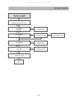
Page 32: ...drive signal input in Q430 base Check H driver B voltage in T802 5 Check IIC bus communication between main assy and ICM2 Check ICM2 40 H drive output 5Vp p 0 7Vp p 12Vp p 2Vp p 6Vp p DC 115V 31 5KHz...

Page 33: ...the TR Check R445 Check F401 High Voltage Generator font Check F401 7 OVP high voltage control oscillating waveform Check R447 Replace I421 No No Yes Q891 Base 0V Horizontal Deflection Check F401 8 HV...

Page 34: ...orm Check I301 5 voltage waveform Check I301 2 vertical deflection waveform Check ICM2 Check vertical B 15V 15V I301 6 I301 1 Check R442 R417 D441 R416 R451 D440 END 50Hz 60Hz 60Hz END 22VP p 22VP p 5...

Page 35: ...by power LED isn t red NO YES YES YES Check IS801 1 DC 7 10V Replace IS801 NO NO Check IS801 1 0V Check DS810 0V Check RS801 is open Replace DS810 YES Check F801 Replace FUSE YES Check Power Code END...

Page 36: ...y circuit Replace QS802 Replace I804 or check DS815 NO Check I801 3 DC 20V Check QS801 DS807 works nomally Check QS801 DS807 works nomally NO Check 2nd power ass y YES Replace I801 YES Change this par...

Page 37: ...M561 4855624200 MARK BRAND AL T1 0 DIA CUTTING LOC PARTCODE PARTNAME DESCRIPTION REMARK ZZ210 PTEGPWG041 ENGINE AS DSJ 4710CRU M961 485961064R PRT P16LSG03RJA M962 485961064G PRT P16LSG03HKA M963 485...

Page 38: ...J 1608 CC182 HCBK103KBA C CHIP CERA 50V X7R 0 01MF K 1608 CC183 HCBK103KBA C CHIP CERA 50V X7R 0 01MF K 1608 CC184 HCBK103KBA C CHIP CERA 50V X7R 0 01MF K 1608 CC185 HCBK152KBA C CHIP CERA 50V X7R 150...

Page 39: ...08 CCM52 HCBK104KBA C CHIP CERA 50V X7R 0 1MF K 1608 CCM53 HCBK104KBA C CHIP CERA 50V X7R 0 1MF K 1608 CCM54 HCBK104KBA C CHIP CERA 50V X7R 0 1MF K 1608 CCM55 HCBH224KBA C CHIP CERA 25V X7R 0 22MF K 1...

Page 40: ...R CHIP 1 10 0 OHM J 1608 LOC PARTCODE PARTNAME DESCRIPTION REMARK RCM44 HRFT000JBA R CHIP 1 10 0 OHM J 1608 RCM45 HRFT102JBA R CHIP 1 10 1K OHM J 1608 RCM47 HRFT100JBA R CHIP 1 10 10 OHM J 1608 RCM48...

Page 41: ...C608 CEXD1E100F C ELECTRO 25V RND 10MF 5X11 TP C609 CEXD1E100F C ELECTRO 25V RND 10MF 5X11 TP C610 CEXF1H100V C ELECTRO 50V RSS 10MF 5X11 TP C650 CEXF1E221V C ELECTRO 25V RSS 220MF 8X11 5 TP LOC PARTC...

Page 42: ...1608 CC666 HCBK104KBA C CHIP CERA 50V X7R 0 1MF K 1608 CCA10 HCBK103KBA C CHIP CERA 50V X7R 0 01MF K 1608 LOC PARTCODE PARTNAME DESCRIPTION REMARK CCA11 HCBK103KBA C CHIP CERA 50V X7R 0 01MF K 1608 CC...

Page 43: ...92 020 0000A 4957002001 HEAT SINK AL EX 0000B 7174301411 SCREW TAPPTITE TT2 RND 3X14 MFZN IA905 PTBASW2001 HEAT SINK ASS Y 1STK392 7174301411 LOC PARTCODE PARTNAME DESCRIPTION REMARK 00001 1STK392 IC...

Page 44: ...L CA156 CCZB1H101K C CERA 50V B 100PF K AXIAL DF419 DRGP15J DIODE RGP15J DO 204AC 600V 1 5A JA115 85801065GY WIRE COPPER AWG22 1 0 65 TIN COATING JA116 85801065GY WIRE COPPER AWG22 1 0 65 TIN COATING...

Page 45: ...4857417500 TERM PIN DA IB0214 D2 3 DY PIN PB906 4857417500 TERM PIN DA IB0214 D2 3 DY PIN LOC PARTCODE PARTNAME DESCRIPTION REMARK PB907 4857417500 TERM PIN DA IB0214 D2 3 DY PIN PB908 4857417500 TER...

Page 46: ...N REMARK R985 RD AZ303J R CARBON FILM 1 6 30K OHM J R986 RD AZ303J R CARBON FILM 1 6 30K OHM J R987 RD AZ224J R CARBON FILM 1 6 220K OHM J R988 RD AZ224J R CARBON FILM 1 6 220K OHM J R989 RD AZ224J R...

Page 47: ...HCBK104KBA C CHIP CERA 50V X7R 0 1MF K 1608 CC559 HCBK104KBA C CHIP CERA 50V X7R 0 1MF K 1608 CC560 HCQK100JBA C CHIP CERA 50V CH 10PF J 1608 CC561 HCBK122KBA C CHIP CERA 50V X7R 1200PF K 1608 CC562 H...

Page 48: ...500MD TO 220AC D475 PTB3SW2000 HEAT SINK ASS Y DFMP3FU 7174300811 00001 DFMP3FU DIODE FMP3FU 0000A 4857032000 HEAT SINK AL PR T1 LOC PARTCODE PARTNAME DESCRIPTION REMARK 0000B 7174300811 SCREW TAPPTIT...

Page 49: ...SR T0 2 R1 6 E42 4856310300 EYE LET BSR T0 2 R1 6 E43 4856310300 EYE LET BSR T0 2 R1 6 E44 4856310300 EYE LET BSR T0 2 R1 6 E45 4856310300 EYE LET BSR T0 2 R1 6 E46 4856310300 EYE LET BSR T0 2 R1 6 E4...

Page 50: ...METAL FILM 2W 100 OHM J SMALL R437 RN02B189JS R METAL FILM 2W 1 8 OHM J SMALL LOC PARTCODE PARTNAME DESCRIPTION REMARK R439 RN02B753JS R METAL FILM 2W 75K OHM J SMALL R440 RN02B132JS R METAL FILM 2W 1...

Page 51: ...OHM J R411 RD 4Z272J R CARBON FILM 1 4 2 7K OHM J R412 RD 4Z152J R CARBON FILM 1 4 1 5K OHM J R414 RD 4Z202J R CARBON FILM 1 4 2K OHM J R415 RD 4Z103J R CARBON FILM 1 4 10K OHM J R423 RD AZ392J R CAR...

Page 52: ...51 8 Schematic Diagram 1 Block Diagram All manuals and user guides at all guides com...

Page 53: ...52 Schematic Diagram 2 Power All manuals and user guides at all guides com...

Page 54: ...53 Schematic Diagram 3 Convergence AMP All manuals and user guides at all guides com...

Page 55: ...54 Schematic Diagram 4 Convergence Module All manuals and user guides at all guides com...

Page 56: ...55 5 CRT Amp Schematic Diagram All manuals and user guides at all guides com a l l g u i d e s c o m...

Page 57: ...56 6 IF Module Schematic Diagram All manuals and user guides at all guides com...

Page 58: ...57 7 AV Main Schematic Diagram All manuals and user guides at all guides com...

Page 59: ...58 8 Micom Module Schematic Diagram All manuals and user guides at all guides com...

Page 60: ...59 9 Control Union Schematic Diagram All manuals and user guides at all guides com...

Page 61: ...60 1 Main PCB 9 PRINTED CIRCUIT BOARD All manuals and user guides at all guides com a l l g u i d e s c o m...

Page 62: ...61 2 Power PCB PRINTED CIRCUIT BOARD All manuals and user guides at all guides com...

Page 63: ...62 3 Convergence Module PCB PRINTED CIRCUIT BOARD All manuals and user guides at all guides com...

Page 64: ...63 4 IF Module PCB PRINTED CIRCUIT BOARD All manuals and user guides at all guides com...

Page 65: ...64 5 CRT PCB PRINTED CIRCUIT BOARD All manuals and user guides at all guides com...

Page 66: ...65 6 UNION PCB PRINTED CIRCUIT BOARD All manuals and user guides at all guides com a l l g u i d e s c o m...

Page 67: ...66 1 DSJ 4710CRU 10 EXPLODED VIEW All manuals and user guides at all guides com...

Page 68: ...67 2 DSJ 4720CRU EXPLODED VIEW All manuals and user guides at all guides com...

Page 69: ...All manuals and user guides at all guides com...

Reviews: