background image


5. Using the Memory Address Map 


ADI16-4(FIT)GY 

51


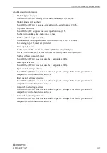
Module Information Area 

The module information area is a 128-byte (80h) area beginning with address 300000h and 
corresponding to a given Device ID. 

The starting address can be determined according to the following expression: 

Starting address

 = 3 80h x (Device ID) 

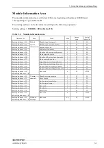
Table 5.3.  Module information area 

Address (h) 

Area 

Item 

Size 

Access 

type 

Initial 

value (h) 

Starting a 00 

Module- 
specific 
information 

Module type (category) 

00 

Starting a 01 

Module type (serial number) 

00 

Starting a 02 

System-reserved 

00 

Starting a 03 

Supported functions 

00 

Starting a 04 

Number of basic input channels 

00 

Starting a 05 

Basic input data size 

00 

Starting a 06 

Number of basic output channels 

00 

Starting a 07 

Basic output data size 

00 

Starting a 08 

Input channel settings address 

00 

Starting a 09 

Input channel settings data size 

00 

Starting a 0A 

Output channel settings address 

00 

Starting a 0B 

Output channel settings data size 

00 

Starting a 0C 
to Starting a 0F 

Reserved 

all 00 

Starting a 10 

Common to 
channels 

Module startup register 

00 

Starting a 11 

Error status 

00 

Starting a 12 

Analog input resolution 

00 

Starting a 13 

Analog input range 

00 

Starting a 14 

Reserved 

00 

Starting a 15 

Gain data  

00 

Starting a 16 

Offset data 

00 

Starting a 17 
to Starting a 1F 

Reserved 

all 00 

Starting a 20 
to Starting a 7F 

Channel 
settings 

Reserved 

96 

all 00 


Summary of Contents for F&eIT Series

Page 1: ...F eIT Series Isolated High Resolution Analog Input Module ADI16 4 FIT GY User s Manual CONTEC CO LTD...

Page 2: ...er Product Configuration List Module ADI16 4 FIT GY 1 First Step Guide 1 CD ROM F eIT Series Setup Disk 1 1 Interface connector plug 1 Warranty Certificate 1 Serial number label 1 1 The CD ROM contain...

Page 3: ...otice All relevant issues have been considered in the preparation of this document Should you notice an omission or any questionable item in this document please feel free to notify CONTEC CO LTD Rega...

Page 4: ...fety Precautions 5 Safety Information 5 Handling Precautions 6 Environment 8 Inspection 8 Storage 8 Disposal 8 2 MODULE NOMENCLATURE AND SETTINGS 9 Nomenclature of Module Components 9 Setting a Device...

Page 5: ...ing Procedure 20 FIFO Function Overview 23 Overview of the Sampling Function 25 List of Commands 36 Examples 37 Software Mode 37 Clock Mode No Interrupts 40 Clock Mode with Interrupts 43 5 USING THE M...

Page 6: ...it to external devices Features Bus isolated analog input module providing high precision at a resolution of 16 bits Selectable input ranges common to channels Bipolar input from 10 to 10 V and curre...

Page 7: ...controller to which the ADI16 4 FIT GYis connected Functions available with each controller connected 1 For the function available refer to the reference manual for the SVR MMF FIT GY 2 Sampling timer...

Page 8: ...I O Address Map Control using the memory address map When connected to the CPU CAxx FIT GY the ADI16 4 FIT GY can be accessed from the host computer over the network The ADI16 4 FIT GY is assigned wit...

Page 9: ...to one year from the date of purchase by the original purchaser Repair will be free of charge only when this device is returned freight prepaid with a copy of the original invoice and a Return Mercha...

Page 10: ...estruction of equipment and resources Understand the meanings of these labels to operate the equipment safely DANGER indicates an imminently hazardous situation which if not avoided will result in dea...

Page 11: ...laim any responsibility for equipment whose casing has been opened To prevent damage please do not subject the module to impact or bend it To prevent contact malfunction please do not touch the metall...

Page 12: ...provide reasonable protection against harmful interference when the equipment is operated in commercial environment This equipment generates uses and can radiate radio frequency energy and if not ins...

Page 13: ...to use it safely Storage When storing this product keep it in its original packing form 1 Put the module in the storage bag 2 Wrap it in the packing material then put it in the box 3 Store the package...

Page 14: ...d keeps track of the modules that are connected to it by assigning device IDs to them Each module therefore should be assigned a unique ID A Device ID can be assigned in a 0 to 7 range so that a maxim...

Page 15: ...t The input range is common to all channels it cannot be set for each of them and must not be set to an invalid range Setup Method To set the voltage or current input use the corresponding DIP switch...

Page 16: ...ting an interface connector and connectors that can be used Removing the connector plug by grasping the cable can break the wire Signal Layout on the Interface Connector The Module can be connected to...

Page 17: ...gher noise immunity Connect the and analog input channels of the Module to the output and ground of the signal source respectively Also connect the analog ground of the Module to the ground of the sig...

Page 18: ...are more than one current source no potential difference must exist between their respective GND points The ADI16 4 FIT GY is isolated between its internal CPU and the external device but not between...

Page 19: ...al Device 14 ADI16 4 FIT GY Converted data is undefined when either of the and input terminals is left unconnected Connect both of the and input terminals of the channel not connected to the signal so...

Page 20: ...them in the appropriate language for the target OS or development system Table 4 1 List of starting I O addresses ID No Occupied I O address 0 0800h to 081Fh recommended 0840h to 085Fh 0880h to 089Fh...

Page 21: ...15 0Fh Analog Input Lower 16 10h Conversion Data7 Conversion Data6 Conversion Data5 Conversion Data4 Conversion Data3 Conversion Data2 Conversion Data1 Conversion Data0 LSB Analog Input Upper 17 11h...

Page 22: ...ta6 Command Data5 Command Data4 Command Data3 Command Data2 Command Data1 Command Data0 25 19h N A 27 1Bh Setting Data 0 28 1Ch Setting Data07 Setting Data06 Setting Data05 Setting Data04 Setting Data...

Page 23: ...ct information Revision Data D3 to D0 This is product update information subject to change without notice that is managed by CONTEC Product Category D7 to D4 This is a module function classification c...

Page 24: ...led Status D6 This bit indicates an interrupt request status in the module When IRQ5 IRQ7 or IRQ9 is 1 this bit will also be 1 IRQ D2 to D0 These bits allow you to verify the interrupt level that is c...

Page 25: ...put Setting Data 0 28 1Ch 0 0 Mode Data1 Mode Data0 0 0 Voltage Curent Gain Offset Input Output EEPROM Data 29 1Dh Calibration Data7 Calibration Data6 Calibration Data5 Calibration Data4 Calibration D...

Page 26: ...8 Setting calibration data Gain Offset D0 Select the calibration data item to be output to the digital potentiometer The data output to the digital potentiometer is cleared the moment the power is tur...

Page 27: ...0 by the following condition Initialization command output Given below are samples for setting calibration data 1 Example to output factory set gain calibration data to the potentiometer outp ADR 24...

Page 28: ...many items of conversion data as the number of data items set in the FIFO Flag register It is cleared by a status reset Calibration Busy D3 See the Calibration Data Setting Procedure section EEPROM Bu...

Page 29: ...f Data5 Number of Data4 Number of Data3 Number of Data2 Number of Data1 Number of Data0 Figure 4 12 Number of data items stored in FIFO memory The following example can be used to check the number of...

Page 30: ...be checked by monitoring the status An interrupt can also be generated as the status changes Figure 4 15 illustrates the analog input procedure The initialization must be performed prior to any sampl...

Page 31: ...lowing are examples of the initialization that is effected outp ADR 24 0x0 Setting calibration data The following example is used to set factory set data For details see the Calibration Data Setting P...

Page 32: ...el mode in which only one channel is specified or the multi channel mode in which two or more channels are specified Channel Mode 0 Single Initialized state 1 Multi Sampling clock D1 This option shoul...

Page 33: ...Range Data 28 1Ch Range Data7 Range Data6 Range Data5 Range Data4 Range Data3 Range Data2 Range Data1 Range Data0 Figure 4 18 Setting an input range Table 4 3 Input range and settings data Range Inpu...

Page 34: ...D4 D3 D2 D1 D0 Output Command 24 18h 0 0 0 0 0 1 0 0 D7 D6 D5 D4 D3 D2 D1 D0 Output Timer Data 0 28 1Ch Timer Data07 Timer Data06 Timer Data05 Timer Data04 Timer Data03 Timer Data02 Timer Data01 Timer...

Page 35: ...mpling mode set to the clock mode and then the sampling process is restarted any conversion data that has accumulated up to that point and the analog input status are reset and a new sampling operatio...

Page 36: ...D1 D0 Input Analog Input Lower 16 10h Conversion Data7 Conversion Data6 Conversion Data5 Conversion Data4 Conversion Data3 Conversion Data2 Conversion Data1 Conversion Data0 LSB Analog Input Upper 17...

Page 37: ...e conversion data is stored this status is set to 1 In the case of the multi channel mode this status is set to 1 when conversion data equal to the number of specified channels is available When reada...

Page 38: ...OM Busy see the Calibration Data Setting Procedure section Details on Resetting the Status This step clears the analog input status Starting I O address D7 D6 D5 D4 D3 D2 D1 D0 Output Analog Input Sta...

Page 39: ...unction Status Explanation Data Read Enable Data Read Enable status set Data Over Error Data Overwrite Error status set Sampling Clock Input Sampling clock is input internally Sampling Clock Error Sam...

Page 40: ...6 D5 D4 D3 D2 D1 D0 Interrupt Mask0 28 1Ch 1 1 Setting Clock Error Sampling Clock Input 1 Data Over Write Error 1 Data Read Enable Interrupt Mask1 29 1Dh 1 1 1 FIFO Memory Flag 1 1 1 1 Figure 4 25 Int...

Page 41: ...tion Data length 00 0 Initialization 0 bit 01 1 Interrupt source mask 8 bit 02 2 Sampling settings 8 bit 03 3 Input range 8 bit 04 4 Internal sampling clock 32 bit 05 5 Timer start 0 bit 06 6 Timer st...

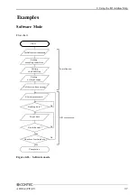
Page 42: ...4 26 Software mode Yes Yes No No Yes No Input data Initialization command Setting an input range Starting command Final channel Number of setting data Initialization A D comversion Setting the FIFO fl...

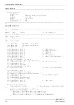
Page 43: ...1c 0x00 10 to 10V outp ADR 0x18 0xb Factory Setting Gain outp ADR 0x1c 0x20 while inp ADR 0x17 0x4 GainData unsigned char inp ADR 0x1c outp ADR 0x18 0xa set Gain Data outp ADR 0x1c 0x0 outp ADR 0x1d G...

Page 44: ...4 Using the I O Address Map ADI16 4 FIT GY 39 printf n End of file...

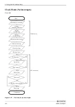
Page 45: ...o Yes No Timer stop Input data Starting timer Channel setting Clock data setting Status reset Yes No Loading data Clock error Initialization command Setting an input range Final channel Number of sett...

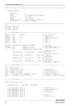
Page 46: ...0x18 0x02 Sampling Mode outp ADR 0x1c 0x05 Clock outp ADR 0x18 0x07 FIFO Flag outp ADR 0x1c 0x20 outp ADR 0x18 0x03 Range outp ADR 0x1c 0x00 10 to 10V outp ADR 0x18 0xb Factory Setting Gain outp ADR...

Page 47: ...s 0x01 for j 0 j 4 j LowerData unsigned char inp ADR 0x10 UpperData unsigned char inp ADR 0x11 VDAT unsigned int UpperData 0x100 LowerData 20 0f 65536 0f 10 0f printf 01dch Input Data 02x 02x Input Vo...

Page 48: ...o No Yes No Return Data display Completion of interrupt Returning of interrupt vector Completion of interrupt Counting the number of interrupt EOI No Yes Changing of interrupt vector Removing interrup...

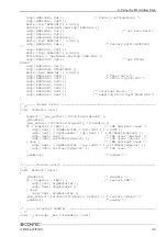
Page 49: ...rImr OrgSlaveImr original IMR unsigned char IntVector 3 0x0d 0x0f 0x71 interrupt vector unsigned char PicMask 3 0xdf 0x7f 0xfd mask bit unsigned char IsrClear 3 0x65 0x67 0x61 ISR clear unsigned char...

Page 50: ...p ADR 0x18 0x01 Interrupt Factor outp ADR 0x1c 0xef Sampling Clock Input Mask OFF change vector void ChgVect void OrgVect _dos_getvect IntVector IrqLevel _disable _dos_setvect IntVector IrqLevel intha...

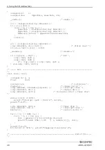
Page 51: ...outp 0xa0 0x20 outp 0xa0 0x0b if inp 0xa0 outp 0x20 0x20 else outp 0x20 0x20 main void main void unsigned int i j float Volt Initialize initialize ChgVect change vector outp ADR 0x2 IntEnable IrqLevel...

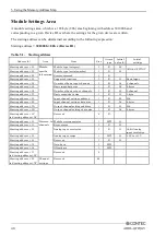
Page 52: ...ller Module manual Following is an explanation of the memory areas necessary for the use of the ADI16 4 FIT GY the module settings area the module information area and the basic input data area Module...

Page 53: ...address 05 Basic input data size 1 R 02 2 bytes Starting address 06 Number of basic output channels 1 R 00 0 channel Starting address 07 Basic output data size 1 R 00 0 byte Starting address 08 Input...

Page 54: ...bits are used by the ADI16 4 FIT GY Number of basic output channels The ADI16 4 FIT GY does not take basic output data 00h Basic input data size The ADI16 4 FIT GY does not take basic output data 00h...

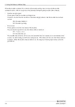
Page 55: ...e not reflected in the module settings area always remain 00h The error status on a module is stored in the module information area Analog input resolution The analog input resolution capacity of the...

Page 56: ...ic input data size 1 R 00 Starting address 06 Number of basic output channels 1 R 00 Starting address 07 Basic output data size 1 R 00 Starting address 08 Input channel settings address 1 R 00 Startin...

Page 57: ...ly indicates that the module has not been started 00h Module shutdown 01h Module operating Error status This register stores the error status of the module The error status register is reset when the...

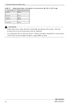
Page 58: ...address 06 CH3 Analog input value 2 R Starting address 08 to Starting address 7F Reserved 120 Analog input value Analog input values are stored as Little Endians Table 5 5 Analog input value D7 D6 D5...

Page 59: ...00030V 8001h 0 00000V 8000h 0 00030V 7FFFh 10 00000V 0000h Analog input values contain data that is valid during the operation of the module When the module is shut down the analog input values are u...

Page 60: ...Yes No Error status can be checked by reading address 300011h Determine category by reading address 301000h For analog type module category is 02h Set analog input range Analog input range is written...

Page 61: ...rmation Common define FIT_PRODUCT_DIGITAL 0x01 define FIT_PRODUCT_ANALOG 0x02 define FIT_PRODUCT_COUNTER 0x03 define FIT_MODULE_START_OFF 0x00 define FIT_MODULE_START_ON 0x01 Address AIO define FIT_AI...

Page 62: ...tus FIT_Close hHandle return 1 if byCategory FIT_PRODUCT_ANALOG printf Error Category 02X H n byCategory FIT_Close hHandle return 1 Write A D Range byRange FIT_AIO_RANGE_PM10 Range 10 to 10V wStatus F...

Page 63: ...dwVaBase FIT_IO FIT_IO_DEVICE_INFOR wStatus FIT_Read hHandle dwVaBase dwVaOffset FIT_ERROR_STATUS 1 byErrorStatus if wStatus 0 printf Error FIT_Read 04X H n wStatus if byErrorStatus 0x00 printf Error...

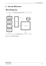
Page 64: ...stem Reference Block Diagram Figure 6 1 Circuit block diagram Stack Connector Control Circuit Device ID Interface Connector CH0 to CH3 Isolator 4 channel Multiplexer with Voltage Protection Instrument...

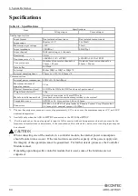
Page 65: ...tion to 35mm DIN rails standard connection mechanism provided in the system Compatible wires AWG28 to 16 Cross section 0 08 to 1 25mm Connectors FK MC1 5 12 STF 3 81 plug made by Phoenix Contact Corp...

Page 66: ...6 2 Installation Environment Requirements Parameter Requirement description Operating temperature 0 to 50 C Storage temperature 10 to 60 C Humidity 10 to 90 RH No condensation Floating dust particles...

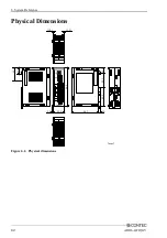
Page 67: ...6 System Reference 62 ADI16 4 FIT GY Physical Dimensions Figure 6 2 Physical dimensions 1 2 94 0 25 2 64 7 4 0 3 5 1 2 mm CH0 CH1 CH2 CH3 AG AG AG AG 14 0 35 0 45 0 14 0 31 5...

Page 68: ......

Page 69: ...31 Himesato Nishiyodogawa ku Osaka 555 0025 Japan https www contec com No part of this document may be copied or reproduced in any form by any means without prior written consent of CONTEC CO LTD 0831...

Reviews: