


6
LED Fusing Considerations
Although the average current draw per module is very low, due to the type of circuit used to power each module, the instantaneous
peak current to a module can be significantly higher during low voltage conditions. To avoid prematurely blowing ATO style fuses
or tripping breakers it is recommended the following rule-of-thumb be used to size fuses or breakers. This is especially important in
lightbars with many LED modules running off a single fused source.
Minimum fuse size calculation: (See Wiring Diagram page 5)
For LED 12 volt electrical current
1.5 X (number of 6LED modules being fused) + .5 X (number of 3LED modules being fused) = Total Electrical Current at 12.8 VDC
LED MODULES
Operating Specifications for directional module:
Operating Voltage:
10-16 VDC, Reverse Polarity Protection
Current Draw :
Flashing Module
Red/Amber - .25A avg @ 12.8 Volts
Blue/White - .4A avg @ 12.8 Volts
Steady Burn Module
Red/Amber - .5A avg @ 12.8 Volts
Blue/White - .8A avg @ 12.8 Volts
Available Colors -
Red , Blue, Amber, and White
This Product contains high intensity TriCore® devices. To prevent eye
damage, DO NOT stare into light beam at close range.
WARNING!
Flash Pattern Changes
LED Lighthead Flash Pattern
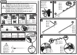
Place the unit on a clean work surface and remove the outer cover. With the chassis facing up, locate each lighthead mod-
ule circuit board.
To change the flash patterns of the LED Lightheads, touch both posts of the J1 header simultaneously
with an electrically conductive tool such as a screw driver blade (see Figure 13 below). Repeating this proceedure allows
the operator to cycle through the numerous flash patterns offered until the desired pattern is achieved.
Directional module Flash Pattern
CycleFlash (DEFAULT)
Quad Pop Flash75
NFPA QuadFlash75
Triple Pop Flash75
Steadyburn
SingleFlash375
ModelFlash
SingleFlash250
ActiveFlash
SingleFlash150
FiveFlash70
FiveFlash150
QuadFlash70
QuadFlash150
TripleFlash70
DoubleFlash150
DoubleFlash70
TripleFlash150
SingleFlash75
Flash Pattern Header for OPTIX
J1
Momentarily short and release
to change patterns
PCB
FIGURE 13