background image


CMT2380F17 

Rev0.1 | 158/347


www.cmostek.com 


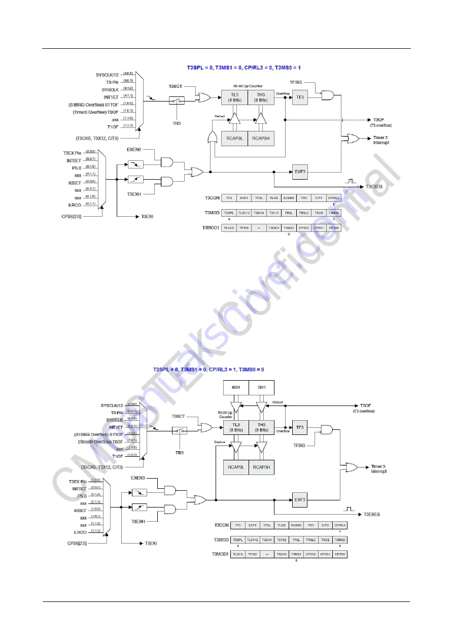
Figure 16-28. Timer 3 Mode 1 Structure (Auto-Reload with External Interrupt Mode) 

16.3.3


Timer 3 Mode 2 (Capture) 

Figure  16

–29  shows  the  capture  mode  there  are  two  options  selected  by  bit  EXEN3  in  T3CON.  If 

EXEN3=0, Timer 3 is a 16-bit timer or counter which, upon overflow, sets bit TF3 (Timer 3 overflow flag). This 
bit  can  then  be  used  to  generate  an  interrupt  (by  enabling  the  Timer  3  interrupt  bit  in  the  EIE2  register).  If 
EXEN3=1, Timer 3 still does the above, but with the added feature that a 1-to-0 transition at T3EXI, one of 8 
Timer 3 external inputs, that causes the current value in the Timer 3 registers, TH3 and TL3, to be captured 
into  registers  RCAP3H  and  RCAP3L,  respectively.  In  addition,  the  transition  at  T3EXI  causes  bit  EXF3  in 
T3CON to be set, and the EXF3 bit (like TF3) can generate an interrupt which vectors to the same location as 
Timer 3 overflow interrupt. T3EXH performs the same function as EXEN3 but it enables the detecting a 0-to-1 
transition at T3EXI input. 


Figure 16-29.    Timer 3 Mode 2 Structure (Capture Mode) 

Summary of Contents for CMT2380F17

Page 1: ...an reach 36 MHz Double data pointer Interrupt control 16 interrupt sources 4 priority levels 3 external interrupts nINT0 1 2 with filtering All external interrupts supporting high low or rising fallin...

Page 2: ...of internal high speed low speed low power RC oscillators and 32 768 kHz external crystal oscillators flexible data handling and packet handler up to 64 byte Tx Rx FIFO feature enriched RF GPIO multi...

Page 3: ...20 0402 X7R 25 V 0 1 uF C13 20 0603 X7R 25 V 4 7 uF C14 20 0603 X7R 25 V 1 uF C15 20 0603 X7R 25 V 0 1 uF L1 10 0603 multilayer chip inductor 180 100 100 nH Sunlord SDCL L2 10 0603 multilayer chip ind...

Page 4: ...n 23 1 21 Correlation Among Receive Current Supply Voltage and Temperature 24 1 22 Receive Sensitivity and Supply Voltage Correlation 25 1 23 Receive Sensitivity and Temperature Correlation 25 1 24 Tr...

Page 5: ...ansfer Count Address Pointer 59 8 2 4 Start a DMA Transfer 60 8 2 5 Suspend or Stop DMA Transfer 60 8 2 6 DMA Interrupt 60 8 2 7 DMA Loop Mode 61 8 2 8 Error Handling in DMA 61 8 2 9 Data Copied to CR...

Page 6: ...ructure 95 14 1 8 General Port Digital Input Configured 96 14 1 9 General Push Pull Output Structure 96 14 1 10 Port Pin Output Driving Strength Selection 96 14 1 11 Port Pin Output Fast Driving Selec...

Page 7: ...162 16 3 8 Split Timer 3 Mode 3 Capture with Auto Zero 163 16 3 9 Split Timer 3 Mode 4 8 bit PWM Mode 164 16 3 10 Timer 3 Programmable Clock Output 164 16 3 11 Timer 3 Register 166 16 4 Timer Global...

Page 8: ...1BRG 232 19 2 S1BRG configuration S1TME 0 232 19 2 1 Baud Rate in Mode 0 232 19 2 2 Baud Rate in Mode 2 233 19 2 3 Baud Rate in Mode 1 3 233 19 3 Serial Port 1 Mode 4 SPI Master 236 19 4 8 Bit Timer M...

Page 9: ...ate 284 26 2 5 ADC Interrupts 284 26 2 6 ADC Window Detect 285 26 2 7 ADC Channel Scan Mode 286 26 2 8 Transfer ADC Data by DMA 286 26 2 9 I O Pins Used with ADC Function 287 26 2 10 Idle and Power Do...

Page 10: ...R Bit Assignment Page P 322 30 5 Auxiliary SFR Register 324 31 Hardware Option 333 32 Application Notes 335 32 1 Power Supply Circuit 335 32 2 Reset Circuit 335 32 3 ICP and OCD Interface Circuit 335...

Page 11: ...tion Min Typ Max Supply voltage VDD 0 3 3 6 V Interface voltage VIN 0 3 3 6 V Junction temperature TJ 40 125 Storage temperature TSTG 50 150 Soldering temperature TSDR Lasts for at least 30 seconds 25...

Page 12: ...7 3 mA FSK 915 MHz 10 kbps 10 kHz FDEV 7 6 mA TX current ITx FSK 433 MHz 20 dBm Direct tie 72 mA FSK 433 MHz 20 dBm With RF switch 77 mA FSK 433 MHz 13 dBm Direct tie 23 mA FSK 433 MHz 10 dBm Direct t...

Page 13: ...7 dBm DR 10 kbps FDEV 10 kHz 113 dBm DR 10 kbps FDEV 10 kHz low power configuration 111 dBm DR 20 kbps FDEV 20 kHz 111 dBm DR 20 kbps FDEV 20 kHz low power configuration 109 dBm DR 50 kbps FDEV 25 kHz...

Page 14: ...kHz 109 0 dBm 433 92 MHz DR 100 kbps FDEV 50 kHz 107 8 dBm 433 92 MHz DR 200 kbps FDEV 50 kHz 103 5 dBm 433 92 MHz DR 200 kbps FDEV 100 kHz 104 3 dBm 433 92 MHz DR 300 kbps FDEV 50 kHz 98 0 dBm 433 92...

Page 15: ...S to RX 20 us TTFS RX From TFS to TX 20 us TTX RX From TX to RX Needs 2Tsymbol to ramp down 2Tsymbol 350 us TRX TX From RX to TX 350 us Notes 1 TSLP RX and TSLP TX are dominated by the crystal oscilla...

Page 16: ...CMT2380F17 Rev0 1 16 347 www cmostek com Parameter Symbol Condition Min Typ Max Unit 500 kHz deviation 111 dBc Hz 1MHz deviation 121 dBc Hz 10 MHz deviation 130 dBc Hz...

Page 17: ...l all IO ports VIH1 Except P6 0 and P6 1 0 6 VDD Input high level RST P6 0 P6 1 VIH2 0 75 VDD Input low level all IO ports VIL1 Except P6 0 and P6 1 0 15 VDD Input low level RST P6 0 P6 1 VIL2 0 2 VDD...

Page 18: ...ent IWAT WDT 32KHz ILRCO in power down mode 5 uA Monitor mode operating current IMON BOD1 is enabled in power down mode 10 uA RTC mode operating current IRTC RTC operates in power down mode VDD 3 0V 4...

Page 19: ...by design not from test 2 The data is based on the characteristics not from product test 1 15 Controller Flash Characteristics Parameter Symbol Condition Note Typ Max Unit Supply power voltage TA 40 C...

Page 20: ...DD 2 51K resistor divider 4 1 uS CH0 GND CH1 VDD 2 10K resistor divider 0 6 uS ADC power supply current ADPS 1 0 00 2 3 2 9 mA ADPS 1 0 01 2 2 2 8 mA ADPS 1 0 10 2 1 2 6 mA ADPS 1 0 11 2 2 5 mA Notes...

Page 21: ...Shift Register Mode Timing Waveform 1 19 Controller SPI Timing Characteristics Parameter Symbol Condition Note Typ Max Unit SPICLK High Time tMCKH Master mode timing 1T TSYSCLK SPICLK Low Time tMCKL 1...

Page 22: ...I Master Transfer Waveform with CPHA 0 1 2 3 4 5 6 7 8 SPICLK CPOL 0 SPICLK CPOL 1 Clock Cycle MOSI MISO tCKH tCKL tMIS tMIH tMOH Figure 1 3 SPI Master Transfer Waveform with CPHA 1 SPICLK CPOL 0 SPIC...

Page 23: ...SD tSDZ tSLH SPICLK CPOL 0 SPICLK CPOL 1 Clock Cycle MOSI MISO nSS tSE tCKH tCKL tSIS tSIH tSEZ tSOH Figure1 5 SPI Slave Transfer Waveform with CPHA 1 1 20 Receive Current and Supply Voltage Correlati...

Page 24: ...380F17 Rev0 1 24 347 www cmostek com 1 21 Correlation Among Receive Current Supply Voltage and Temperature Test Conditions Freq 434MHz Fdev 10KHz BR 10Kbps Test Conditions Freq 868MHz Fdev 10KHz BR 10...

Page 25: ...ww cmostek com 1 22 Receive Sensitivity and Supply Voltage Correlation Test Conditions FSK modulation DEV 10KHz BR 10Kbps 1 23 Receive Sensitivity and Temperature Correlation Test Conditions FSK modul...

Page 26: ...Rev0 1 26 347 www cmostek com 1 24 Transmit Power and Supply Voltage Correlation Test Conditions Freq 434 MHz 20 dBm 13 dBm matching network respectively Test Conditions Freq 868MHz 20dBm 13dBm matchi...

Page 27: ...CMT2380F17 Rev0 1 27 347 www cmostek com 1 25 Phase Noise...

Page 28: ...Analog Chip substrate must connect to ground 1 NC No connection 2 3 RFIP RFIN Analog Differential RF signal input port 4 FRO Analog PA output 5 RF AVDD Analog RF circuit VDD requires to connect to a...

Page 29: ...BRG clock output 16 P4 4 IO Port P4 4 OCD_SCL IO Clock signal of OCD debug interface nINT2 I Input signal of external interrupt 2 BEEP O Buzzer output ECI I External clock input of PCA 17 P4 5 IO Port...

Page 30: ...Channel 6 of keyboard input MISO I Signal of SPI module for master input and slave output S0MI I Data input of UART0 SPI master mode PWM0A O Sub channel A of PCA PWM0 module output 27 P1 7 IO Port P1...

Page 31: ...be configured as INT1 INT2 DOUT DIN DCLK TX RX RF_SWT 40 2 GPIO1 IO GPIO1 of RF module it can be configured as DOUT DIN INT1 INT2 DCLK TX RX RF_SWT Notes 1 INT1 and INT2 refer to RF interrupts DOUT re...

Page 32: ...CL P3 1 TWI_SDA P3 0 STWI_SCL nINT1 STWI_SDA S0MI DMA Timer5 Timer6 T5 P3 4 T6 P3 5 UART0 LIN RxD0 P3 0 TxD0 P3 1 S0MI P1 6 T2 T2CKO P1 0 T2EX P1 1 Figure 3 1 Functional System Block Diagram The CMT23...

Page 33: ...dard 80C51 Peripheral CMT2380F17 Peripheral Notes IRAM 256 Bytes 256 Bytes External Interrupt 2 3 Support high low trigger selection Interrupt source 4 Interrupt sources 16 interrupt sources 4 priorit...

Page 34: ...illator and the CPU runs at a particularly slow speed Real time clock RTC mode it supports the real time clock function in all modes Watch mode in power down mode or idle mode WDT overflow is used as...

Page 35: ...rmediate frequency by the quadrature mixer and then filtered by the image rejection filter 3 The signal is further amplified by the limiting amplifier 4 The signal is sent to the digital domain for di...

Page 36: ...the PCB Each pin of the crystal has a 5pF parasitic capacitance inside as an equivalence of 2 5pF altogether The equivalent series resistance of the crystal should meet the specified specifications t...

Page 37: ...reading the register With configuring the value of RSSI_DET_SEL 1 0 users can choose to either output the RSSI value in real time or store RSSI value at each stage during packet receiving The CMT2380F...

Page 38: ...n instance of the internal assisting super low power SLP receive mode In the direct mode the FSK demodulation output can also be muted through setting the DOUT_MUTE register bit to 1based on phase jum...

Page 39: ...K is a serial clock with speed up to 5MHz Data is sent on the falling edge of SCLK and collected on the rising edge for the chip itself or an external MCU SDA is a bidirectional pin for inputting and...

Page 40: ...CLR_TX FIFO_CLR_RX bit and transmit repeated data filled previously by setting FIFO_RESTORE which avoids data refilling When accessing the FIFO users start from configuring a number of registers invol...

Page 41: ...16 RX_FIFO_WBYTE Figure 4 9 Transceiver RX FIFO Interrupt Timing Schematic 1 0 3 2 5 4 7 6 9 8 11 10 13 12 15 14 17 16 19 18 21 20 23 22 25 24 27 26 29 28 31 30 EMPTY FULL TX_FIFO_NMTY TX_FIFO_TH TX_...

Page 42: ...IDLE and resume the power on process any time when reset is performed POR RF VDD POR Release 1 ms XTAL Stablize 2 48 ms Block Calibrations 6 5 ms Enters the SLEEP State Ready for customer initializing...

Page 43: ...he SPI is enabled the registers in the configuration area and control area 1 can be accessed and the contents previously filled in the FIFO is retained but the FIFO cannot be operated If the periodica...

Page 44: ...le In TX users can switch to RX in a prompt way by sending the go_switch command No matter whether the frequency points set by TX and RX are the same it needs to wait for 350us for PLL recalibration a...

Page 45: ...is written in RX FIFO which is a pulse Auto RX_FIFO_OVF 01111 An interrupt indicating RX FIFO overflow Auto TX_FIFO_NMTY 10000 An interrupt indicating TX FIFO is not empty Auto TX_FIFO_TH 10001 An in...

Page 46: ...GPIO2 GPO1_SEL 1 0 GPIO1 0 Preamble OK Interrupt Source 0 Sycn Word OK Interrupt Source 0 Node ID OK Interrupt Source 0 CRC OK Interrupt Source 0 Packet OK Interrupt Source 0 Sleep Timeout Interrupt S...

Page 47: ...ect the current state of the CPU The PSW shown above resides in the SFR space It contains the Carry bit the Auxiliary Carry for BCD operation the two register bank select bits the Overflow flag a Pari...

Page 48: ...0 F SFR Address 0x83 Bit 7 6 5 4 3 2 1 0 Name DPTR 15 8 R W R W ResetV alue 0 0 0 0 0 0 0 0 The DPH register is the high byte of the 16 bit DPTR DPTR is used to access indirectly addressed XRAM and Fl...

Page 49: ...selected bank or the Stack Pointer The address register for 16 bit addresses can only be the 16 bit data pointer register DPTR 5 3 3 Register Instruction REG The register banks containing registers R0...

Page 50: ...ion 0000H where should be the starting of the user s application code To service the interrupts the interrupt service locations called interrupt vectors should be located in the program memory Each in...

Page 51: ...cient use of code space since register instructions are shorter than instructions that use direct addressing The next 16 bytes above the register banks form a block of bit addressable memory space The...

Page 52: ...bytes of XRAM 0000H to 02FFH are indirectly accessed by move external instruction MOVX Ri and MOVX DPTR For C51 compiler to assign the variables to be located at XRAM the pdata or xdata definition sh...

Page 53: ...status registers accessible only via direct addressing xdata External data or on chip eXpanded RAM XRAM duplicates the classic 80C51 64KB memory space addressed via the MOVX DPTR instruction The CMT23...

Page 54: ...te the effective XRAM address 7 1 MOVX on 16 bit Address with dual DPTR The dual DPTR structure as shown in Figure 7 1 is a way by which the chip can specify the address of an external data memory loc...

Page 55: ...esetV alue 0 0 0 0 0 0 0 0 The DPH register is the high byte of the 16 bit DPTR DPTR is used to access indirectly addressed XRAM and Flash memory 7 2 MOVX on 8 bit Address with XRPS The 8 bit form of...

Page 56: ...PS XRAM Page Select The XRPS register provides the high byte of the 16 bit external data memory address when using an 8 bit MOVX command effectively selecting a 256 byte page of RAM Since the upper re...

Page 57: ...CRC engine during DMA transfer Auto initialization for circular buffer management loop mode Capability to suspend and resume a DMA transfer Capability to operate in low power modes idle mode for inte...

Page 58: ...errupt DMA Complete Flag overflow 16 bit Up Counter Current Address TH6 TL6 Base Address THR6 TLR6 reload 16 bit Up Counter 1 65536 bytes Current Transfer Count TH5 TL5 Base Transfer Count THR5 TLR5 D...

Page 59: ...event happened on DMA Current Transfer Count That is one trigger input to activate a block data transfer by DMA controller The block data transfer size is defined in TH5 TL5 as DMA Current Transfer Co...

Page 60: ...trigger wait external active signal to start DMA 8 Software waits DMA Complete Flag DCF0 that indicates the DMA transfer finished 9 Write 0 on DMAE0 to end DMA operation and configure DMADS0 to disab...

Page 61: ...re on A Current Address cannot over the XRAM boundary In CMT2380F17 XRAM boundary is 768 bytes 02FFH B Cannot support the even odd parity check and generation on S0 and S1 C Cannot handle the Not ACK...

Page 62: ...ters If DMA is disabled Timer 6 is a 16 bit auto reloadable timer counter with Gate control function as Timer 0 The overflow flag TF6 could be an interrupt source and shares the DMA interrupt vector F...

Page 63: ...cleared by software writing 0 1 DCF0 is set by DMA end of transfer DMACG0 DMA ConfiGuration Register 0 SFR Page 8 only SFR Address 0x94 Bit 7 6 5 4 3 2 1 0 Name PDMAH PDMAL CRCW0 0 EXTS10 EXTS00 FAEN0...

Page 64: ...ase reference Transfer ADC Data by DMA in ADC Moudle for details 8 4 Timer5 Register T5CON Timer 5 Control Register SFR Page 3 Only SFR Address 0xC8 Bit 7 6 5 4 3 2 1 0 Name TF5 T5CKS1 T5CKS0 T5IE TR5...

Page 65: ...Register SFR Page 3 Only SFR Address 0xCC Bit 7 6 5 4 3 2 1 0 Name TL5 7 0 R W R W R W R W R W R W R W R W R W ResetV alue 0 0 0 0 0 0 0 0 TH5 Timer 5 High byte Register SFR Page 3 Only SFR Address 0...

Page 66: ...W R W R W R W R W R W R W ResetV alue 0 0 0 0 0 0 0 0 Bit 7 TF6 Timer 6 overflow flag 0 TF6 must be cleared by software 1 TF6 is set by a Timer 6 overflow happened Bit 6 Bit 5 4 T6CKS 1 0 Timer 6 cloc...

Page 67: ...Bit 7 6 5 4 3 2 1 0 Name TH6 7 0 R W R W R W R W R W R W R W R W R W ResetV alue 0 0 0 0 0 0 0 0 TLR6 Timer 6 Low byte Reload Register SFR Page 4 Only SFR Address 0xCA Bit 7 6 5 4 3 2 1 0 Name TLR6 7...

Page 68: ...CK 2 and MCK 4 for system application The CMT2380F17 device includes a Clock Multiplier CKM to generate the high speed clock for system clock source CKM applied in CMT2380F17 is shown in Figure 9 1 an...

Page 69: ...ftware need to wait until the clock be settle before switch the clock source 9 3 On chip CKM PLL There are three clock sources for the system clock Internal High frequency RC Oscillator IHRCO Internal...

Page 70: ...S Alternated Frequency Selection 0 Select IHRCO on 12MHz 1 Select IHRCO on 11 059MHz Bit 6 ENCKM Enable clock multiplier X8 X12 0 Disable the X8 X12 clock multiplier 1 Enable the X8 X12 clock multipli...

Page 71: ...k source selection MCKS 1 0 MCK Source Selection OSCin 12MHz CKMIS 01 OSCin 11 059MHz CKMIS 01 CKMS0 0 CKMS0 1 CKMS0 0 CKMS0 1 00 OSCin 12MHz 11 059MHz 01 CKMI x4 x6 24MHz 36MHz 22 118MHz 33 177MHz 10...

Page 72: ...XR0 Auxiliary Register 0 SFR Page 0 F SFR Address 0xA1 Bit 7 6 5 4 3 2 1 0 Name P60OC 1 0 P60FD PBKF INT1H INT0H R W R W R W R W R W W W R W R W ResetV alue 0 0 0 X X X 0 0 Bit 7 6 P6 0 function confi...

Page 73: ...CPU running in lower speed mode FCPUCLK 6MHz which is slow down internal circuit to reduce power consumption 1 Enable CPU full speed operation if FCPUCLK 6MHz Before select high frequency clock 6MHz o...

Page 74: ...write on ENW which will clear the ENW bit The WDTCR register will keep the previous programmed value unchanged after hardware RST pin reset software reset and WDT reset WREN NSW and ENW are implement...

Page 75: ...ared by software in page 0 F In page P software can modify it to 0 or 1 Bit 5 ENW Enable WDT 0 Disable WDT running This bit is only cleared by POR 1 Enable WDT while it is set Once ENW has been set it...

Page 76: ...0 1 4 0 25 ms 120us 0 1 0 8 0 5 ms 120us 0 1 1 16 1 ms 120us 1 0 0 32 2 ms 120us 1 0 1 64 4 ms 120us 1 1 0 128 8 ms 120us 1 1 1 256 16 ms 120us Note 1 When WDT clock source is ILRCO the WDT internal...

Page 77: ...are writing 0 is no operation 1 This bit is only set by hardware when WDT overflows Writing 1 on this bit will clear WDTF SFIE System Flag Interrupt Enable Register SFR Page 0 F SFR Address 0x8E Bit 7...

Page 78: ...for writing of software 11Real Time Clock RTC System Timer The CMT2380F17 has a simple Real Time clock that allows a user to continue running an accurate timer while the rest of the device is powered...

Page 79: ...Real Time Clock Counter RTCCR Real Time Clock Control Register SFR Page 0 7 P SFR Address 0xBE 0x54 Bit 7 6 5 4 3 2 1 0 Name RTCE RTCO RTCRL 5 0 R W R W R W R W R W R W R W R W R W ResetV alue 0 0 1 1...

Page 80: ...n or System Timer function by different clock source selection on RTCCS 1 0 When the counter overflows it sets the RTCF flag which shares the system flag interrupt when RTCFIE is enabled The maximum R...

Page 81: ...s only set by hardware when RTCCT overflows Writing 1 on this bit will clear RTCF SFIE System Flag Interrupt Enable Register SFR Page 0 F SFR Address 0x8E Bit 7 6 5 4 3 2 1 0 Name SIDFIE RTCFIE BOF1IE...

Page 82: ...and indicating flags 12 1 Reset Source Power On Reset External Reset Software Reset Illegal Addr Reset Internal Reset BOD0 Triggered BO0RE PCON2 1 BOD1 Triggered BO1RE PCON2 3 WDT Overflow Brown Out...

Page 83: ...ut reset software reset ISPCR 5 and WDT reset It helps users to check if the running of the CPU begins from power up or not Note that the POF0 must be cleared by firmware Note POF0 must be cleared by...

Page 84: ...it must be cleared by software writing 1 on it Software writing 0 is no operation 1 This bit is only set by hardware if a Software Reset occurs Writing 1 on this bit will clear SWRF 12 5 Brown Out Res...

Page 85: ...that causes CPU to restart Software can read the WDTF to recognize the WDT reset occurred PCON1 Power Control Register 1 SFR Page 0 F P SFR Address 0x97 Bit 7 6 5 4 3 2 1 0 Name SWRF EXRF RTCF BOF1 BO...

Page 86: ...of ESF EIE1 3 and BOF0IE SFIE 1 are enabled a set BOF0 will generate a system flag interrupt It can interrupt CPU either CPU in normal mode or idle mode The BOD1 has the same flag function BOF1 and s...

Page 87: ...DTF and wakeup CPU from interrupt or system reset by software configured The maximum wakeup period is about 2 seconds that is defined by WDT pre scaler Please refer Section 10 Watch Dog Timer WDT and...

Page 88: ...lowing conditions has occurred Start of code execution after any type of reset or Exit from power down mode To ensure minimum power consumption in power down mode software must confirm all I O not in...

Page 89: ...pin must be held high for longer than the timeout period to ensure that the device is reset properly The device will begin executing once RST is brought low It should be noted that when idle is termi...

Page 90: ...curs Bit 6 EXRF External Reset Flag 0 This bit must be cleared by software writing 1 to it 1 This bit is set by hardware if an External Reset occurs Bit 4 RTCF RTC overflow flag 0 This bit must be cle...

Page 91: ...tored level Selection BO1S 1 0 BOD1 detecting level 0 0 2 0V 0 1 2 4V 1 0 3 7V 1 1 4 2V Bit 3 BO1RE BOD1 Reset Enabled 0 Disable BOD1 to trigger a system reset when BOF1 is set 1 Enable BOD1 to trigge...

Page 92: ...dress 0x45 POR 0xxx xxxx Bit 7 6 5 4 3 2 1 0 Name IVREN R W R W R W R W R W R W R W R W R W ResetV alue 0 X X X X X X X Bit 7 IVREN Internal Voltage Reference Enable 0 Disable on chip IVR 1 4V 1 Enabl...

Page 93: ...his is possible because when the port outputs a logic high it is weakly driven allowing an external device to pull the pin low When the pin outputs low it is driven strongly and able to sink a large c...

Page 94: ...Output 14 1 3 Port 3 Input Only High Impedance Input Structure The input only configuration on Port 3 is an input without any pull up resistors on the pin as shown in Figure 14 3 Port Pin Input data...

Page 95: ...O Disabled Analog Input Figure 14 5 General Analog Input Only 14 1 6 General Open Drain Output with Pull up Resistor Structure The open drain output with pull up resistor configuration on general por...

Page 96: ...VDD Figure 14 8 General Push Pull Output 14 1 10 Port Pin Output Driving Strength Selection The I O of the CMT2380F17 has two driving strength can be selected for different kinds of the application to...

Page 97: ...ing to analog input only on these port pins after system reset Figure 14 2 General Port Configuration Settings PxM0 y PxM1 y Port Mode 0 1 Analog Input Only default 1 1 Open Drain with Pull up resisto...

Page 98: ...3 2 1 0 Name P1M1 7 P1M1 6 P1M1 5 P1M1 1 P1M1 0 R W R W R W R W R W R W R W R W R W ResetV alue 1 1 1 1 1 1 1 1 14 2 2 Port 2 Register P2 Port 2 Register SFR Page 0 F SFR Address 0xA0 Bit 7 6 5 4 3 2...

Page 99: ...5 P3 4 P3 3 P3 1 P3 0 R W W W R W R W R W W R W R W ResetV alue 1 1 1 1 1 1 1 1 Bit 5 4 3 1 0 Port 3 output data is set cleared by the CPU P3M0 Port 3 Mode Register 0 SFR Page 0 F SFR Address 0xB1 Bi...

Page 100: ...4 R W R W W R W R W W W W W ResetV alue 1 X 1 1 X X 1 1 Bit 7 0 Port 4 output data latch could be set cleared by CPU P4 5 and P4 4 have the alternated function for OCD_SDA and OCD_SCL Due to MG82F6D17...

Page 101: ...Address 0x92 Bit 7 6 5 4 3 2 1 0 Name P6M1 1 P6M1 0 R W W W W W W W R W R W ResetV alue 1 1 1 1 1 1 1 1 14 2 6 Port Output Driving Strength Control Register In CMT2380F17 all port pins have two drivin...

Page 102: ...e P2 3 P2 0 output with high driving strength 1 Select the P2 3 P2 0 output with low driving strength Bit 3 P1DC1 Port 1 output driving strength control on high nibble 0 Select the P1 7 P1 4 output wi...

Page 103: ...0 reserved bit When writing the PDRVC1 register the software bit must write to 0 14 2 7 Port Output Fast Driving Control Register In CMT2380F17 all port pins have two driving speed selection by softwa...

Page 104: ...st driving on port pin output P4FDC Port 4 Fast Driving Control Register SFR Page A only SFR Address 0x92 Bit 7 6 5 4 3 2 1 0 Name P4FDC 5 P4FDC 4 R W W W R W R W W W W W ResetV alue 0 0 0 0 0 0 0 0 B...

Page 105: ...efault driving 1 P6 0 output with fast driving enabled If P6 0 is configured to clock output enable this bit when P6 0 output frequency is more than 12MHz at 5V application or more than 6MHz at 3V app...

Page 106: ...3 2 1 0 Name C0IC4S0 C0IC2S0 C0PPS1 C0PPS0 C0PS0 ECIPS0 C0COPS R W R W R W R W R W R W R W R W R W ResetV alue 0 0 0 0 0 0 0 0 Bit 7 C0IC4S0 PCA0 Input Channel 4 input port pin Selection C0IC4S0 CEX4...

Page 107: ...BI6PS0 KBI2PS0 T3FCS T2FCS SnMIPS S0COPS R W R W R W R W R W R W R W R W R W ResetV alue 0 0 0 0 0 0 0 0 Bit 7 6 KBI4PS1 0 KBI4 5 Port pin Selection 1 0 KBI4PS1 0 KBI4 KBI5 00 P3 3 P1 5 01 P3 4 P3 5 1...

Page 108: ...Address 0xA4 Bit 7 6 5 4 3 2 1 0 Name POE7 POE6 C0PPS2 KBI0PS0 S1COPS R W R W R W R W W R W R W W W ResetV alue 1 1 0 0 0 0 0 0 Bit 7 POE7 PCA0 PWM7 main channel PWM7O output control 0 Disable PWM7O...

Page 109: ...CMT2380F17 Rev0 1 109 347 www cmostek com Bit 1 0 S1PS1 0 Serial Port 1 pin Selection 1 0 S1PS1 S1PS0 RxD1 TxD1 00 P1 0 P1 1 01 P6 0 P6 1 10 P4 4 P4 5 11 P3 4 P3 5...

Page 110: ...0 Selected Port Pin of nINT1 000 P3 3 001 P3 1 010 P3 5 011 P1 0 100 P6 1 101 P3 4 110 P1 5 111 P2 4 Bit 5 4 INT0IS 1 0 nINT0 input port pin selection bits which function is defined with INT0IS 2 as f...

Page 111: ...CMT2380F17 Rev0 1 111 347 www cmostek com INT2IS 1 0 Selected Port Pin of nINT2 00 P4 4 01 P3 0 10 P1 1 11 P1 6...

Page 112: ...iority level for each interrupt The Priority within Level is the polling sequence used to resolve simultaneous requests of the same priority level The Vector Address is the entry point of an interrupt...

Page 113: ...F ADCON0 ADCI IE1 PCA0 Interrupt Flags System Flags KBCON KBIF SICON SI S1CON RI1 S1CON TI1 T3CON TF3 T3CON EXF3 DMA Flags Highest Priority Level Interrupt Interrupt Polling Sequence IP0L IP0H EIP1L E...

Page 114: ...UXR2 6 AUXR0 2 AUXR0 3 S0CON 1 11 Keypad Interrupt KBIF KBCON 0 12 TWI0 I2C0 SI SICON 3 13 Reserved 14 Serial Port 1 RI1 TI1 S1CON 0 S1CON 1 15 Reserved 16 Timer 3 TF3 EXF3 TF3L T3CON 7 T3CON 6 T3CON...

Page 115: ...If the timer 3 in split mode the TL3 overflow will set another interrupt flag TF3L Just the same as serial port neither of these flags is cleared by hardware when the service routine is vectored to SP...

Page 116: ...et by Keypad module meets the input pattern It will not be cleared by hardware when the service routine is vectored to The TWI0 I2C0 interrupt is generate by SI in SICON which is set by TWI0 I2C0 engi...

Page 117: ...led by their corresponding enable bits If EA is cleared to 0 all interrupts are disabled 15 4 Interrupt Priority The priority scheme for servicing the interrupts is the same as that for the 80C51 exce...

Page 118: ...s An interrupt of equal or higher priority level is already in progress The current cycle polling cycle is not the final cycle in the execution of the instruction in progress The instruction in progre...

Page 119: ...w cmostek com 15 6 nINTx Input Source Selection and input filter x 0 2 The CMT2380F17 provides flexible nINT0 nINT1 and nINT2 source selection to share the port pin inputs Figure 15 2 Configuration of...

Page 120: ...e to specify falling edge triggered external interrupt 1 nINT1 If INT1H AUXR0 1 is set this bit specifies rising edge triggered on nINT1 Bit 1 IE0 Interrupt 0 nINT0 Edge flag 0 Cleared when interrupt...

Page 121: ...t Bit 4 ES Serial port 0 interrupt UART0 enable register 0 Disable serial port 0 interrupt 1 Enable serial port 0 interrupt Bit 3 ET1 Timer 1 interrupt enable register 0 Disable Timer 1 interrupt 1 En...

Page 122: ...R W W W W W R W R W R W R W ResetV alue 0 0 0 0 0 0 0 0 Bit 3 INT2H nINT2 High Rising trigger enable 0 Maintain nINT2 triggered on low level or falling edge on selected port pin input 1 Set nINT2 trig...

Page 123: ...Timer 0 interrupt priority H register Bit 0 PX0H external interrupt 0 priority H register EIE1 Extended Interrupt Enable 1 Register SFR Page 0 F SFR Address 0xAD Bit 7 6 5 4 3 2 1 0 Name ETWI0 EKB ES...

Page 124: ...UART1 interrupt priority L register Bit 3 PSFL system flag interrupt priority L register Bit 2 PPCAL PCA0 interrupt priority L register Bit 1 PADCL ADC interrupt priority L register Bit 0 PSPIL SPI i...

Page 125: ...terrupt priority L register EIP2H Extended Interrupt Priority 2 High Register SFR Page 0 F SFR Address 0xA7 Bit 7 6 5 4 3 2 1 0 Name PT3H R W W W W W W W W R W ResetV alue 0 0 0 0 0 0 0 0 Bit 7 1 Rese...

Page 126: ...s nINT2 input filter mode with X2FLT1 XICFG1 2 X2FLT1 X2FLT nINT2 input filter mode 00 Disabled 01 SYSCLK x 3 10 SYSCLK 6 x 3 11 S0TOF x 3 Bit 1 X1FLT nINT1 Filter mode control It selects nINT1 input...

Page 127: ...XICFG description for nINT1 input filter mode definition Bit 0 X0FLT1 nINT0 Filter mode control It selects nINT0 input filter mode with X0FLT XICFG 0 Refer XICFG description for nINT0 input filter mod...

Page 128: ...this bit will clear RTCF Bit 3 Reserved Software must write 0 on this bit when PCON1 is written Bit 2 BOF1 Brown Out Detection flag 1 0 This bit must be cleared by software writing 1 to it 1 This bit...

Page 129: ...m Bit 6 STOF Stop Flag detection of STWI SID 0 Clear by firmware by writing 0 on it 1 Set by hardware to indicate the STOP condition occurred on STWI bus STOF might be held within MCU reset period so...

Page 130: ...or T3 In this function the external input is sampled by every timer rate cycle When the samples show a high in one cycle and a low in the next cycle the count is incremented The new count value appear...

Page 131: ...CMT2380F17 Rev0 1 131 347 www cmostek com Figure 16 1 Timer 0 Mode 0 Structure Figure15 2 Timer 1 Mode 0 Structure...

Page 132: ...Timer 0 1 in Mode1 is configured as a 16 bit timer or counter The function of GATE TxG1 and TRx is same as mode 0 Figure 16 3 and Figure 16 4 show the mode 1 structure of Timer 0 and Timer 1 Figure 6...

Page 133: ...d Overflow from TLx not only set TFx but also reload TLx with the content of THx which is determined by software The reload leaves THx unchanged Mode 2 operation is the same for Timer0 and Timer1 Figu...

Page 134: ...ammable Clock Out Timer 0 and Timer 1 have a Clock Out Mode while TxCKOE 1 In this mode Timer 0 or Timer 1 operates as 8 bit auto reload timer for a programmable clock generator with 50 duty cycle The...

Page 135: ...ock out equation Note 1 Timer 0 1 overflow flag TF0 1 will be set when Timer 0 1 overflows 2 For SYSCLK 12MHz and select SYSCLK 12 as Timer 0 1 clock source Timer 0 1 has a programmable output frequen...

Page 136: ...Timer 1 So software usually disables the Timer 0 1 interrupt in this kind of application 16 1 6 Timer 0 1 Register TCON Timer Counter Control Register SFR Page 0 F SFR Address 0x88 Bit 7 6 5 4 3 2 1 0...

Page 137: ...eload for Timer1 11 Timer Counter1 Stopped Bit 3 T0GATE Gating control for Timer0 T0G1 T0GATE T0 Gate source 0 0 Disable 0 1 INT0 active 1 0 TF2 active 1 1 KBI active Bit 2 T0C T Timer 0 clock source...

Page 138: ...0 1 138 347 www cmostek com ResetV alue 0 0 0 0 0 0 0 0 TL1 Timer 1 High byte Register SFR Page 0 F SFR Address 0x8B Bit 7 6 5 4 3 2 1 0 Name TL1 7 0 R W R W R W R W R W R W R W R W R W ResetV alue 0...

Page 139: ...clock source selection with T1C T control T1X12 T1C T Timer 1 Clock Selection 0 0 SYSCLK 12 0 1 T1 Pin 1 0 SYSCLK 1 1 SYSCLK 48 Bit 2 T0X12 T0XL and T0C T together control the timer 0 clock source sel...

Page 140: ...SFR Page 1 only SFR Address 0xA4 Bit 7 6 5 4 3 2 1 0 Name T2PS1 T2PS0 T1PS1 T1PS0 R W R W R W R W R W W W W W ResetV alue 0 0 0 0 0 0 0 0 Bit 5 4 T1PS1 0 Timer 1 Port pin Selection 1 0 T1PS1 0 T1 T1CK...

Page 141: ...oad timer counter The TF2 Timer 2 overflow flag is one of the Timer 2 interrupt source which interrupt function can be blocked by TF2IG EXEN2 enables a 1 to 0 transition at T2EXI to set the flag EXF2...

Page 142: ...registers to be reloaded with the 16 bit value in RCAP2L and RCAP2H The values in RCAP2L and RCAP2H are preset by firmware If EXEN2 1 then a 16 bit reload can be triggered either by an overflow or by...

Page 143: ...2 still does the above but with the added feature that a 1 to 0 transition at T2EXI one of 8 Timer 2 external inputs that causes the current value in the Timer 2 registers TH2 and TL2 to be captured i...

Page 144: ...milar function with Timer 2 Mode 2 There is one difference that the T2EXES EXF2 event set signal not only is the capture source of Timer 2 but also clears the content of TL2 and TH2 to 0x0000H Timer 2...

Page 145: ...2 And TH2 overflow can stop the TR2L running when TR2LC is set There are 3 interrupt flags in split mode EXF2 TF2 and TF2L EXF2 has the same function as 16 bit mode to detect the transition on T2EXI T...

Page 146: ...AR with Ex INT When T2SPL is set in this mode Timer 2 is split to two 8 bit timers as shown in Figure 16 17 It is similar function as Timer 2 Mode 1 and keeps the same interrupt scheme in Split Timer...

Page 147: ...er 2 Mode 2 Capture When T2SPL is set in this mode Timer 2 is split to two 8 bit timers as shown in Figure 16 18 It is similar function as Timer 2 Mode 2 and keeps the same interrupt scheme in Split T...

Page 148: ...th Auto Zero When T2SPL is set in this mode Timer 2 is split to two 8 bit timers as shown in Figure 16 19 It is similar function as Timer 2 Mode 3 and keeps the same interrupt scheme in Split Timer 2...

Page 149: ...Timer 2 is used as the serial port transmit baud rate generator RCLK has the same effect for the serial port receive baud rate With these two bits the serial port can have different receive and transm...

Page 150: ...not be written to because a write might overlap a reload and cause write and or reload errors The timer should be turned off clear TR2 before accessing the Timer 2 or RCAP2 registers Note Refer to Sec...

Page 151: ...s of RCAP2H RCAP2L are loaded into TH2 TL2 for the consecutive counting Figure 16 23 gives the formula of Timer 2 clock out frequency Figure 16 24 shows the clock structure of Timer 2 T2 Clock Frequen...

Page 152: ...will be blocked by TF2IG If Timer 2 in split mode the clock output function is generated by TL2 overflow and the output clock frequency is TL2 overflow rate 2 RCAP2L is the TL2 s reload value when TL2...

Page 153: ...7 6 5 4 3 2 1 0 Name TF2 EXF2 RCLK TF2L TCLK TL2IE EXEN2 TR2 C T2 CP RL2 R W R W R W R W R W R W R W R W R W ResetV alue 0 0 0 0 0 0 0 0 Bit 7 TF2 Timer 2 overflow flag 0 TF2 must be cleared by softwa...

Page 154: ...control bit If in Timer 2 split mode it only controls the TH2 0 Disabled to stop the Timer Counter 2 1 Enabled to start the Timer Counter 2 Bit 1 C T2 Timer 2 clock or counter source selector The fun...

Page 155: ...uto Reload and External Interrupt 0 0 1 Mode 1 Auto Reload with External Interrupt 0 1 0 Mode 2 Capture mode 0 1 1 Mode 3 Capture with Auto Zero 1 0 0 Mode 4 8 bit PWM if T2SPL 1 Others Reserved T2MOD...

Page 156: ...er SFR Page 0 Only SFR Address 0xCA Bit 7 6 5 4 3 2 1 0 Name RCAP2 7 0 R W R W R W R W R W R W R W R W R W ResetV alue 0 0 0 0 0 0 0 0 RCAP2H Timer 2 Capture High byte Register SFR Page 0 Only SFR Add...

Page 157: ...same function as EXEN3 but it enables the detecting a 0 to 1 transition at T3EXI input The Timer 3 overflow event T3OF in this module will be output to other peripheral as clock input or event source...

Page 158: ...t in the EIE2 register If EXEN3 1 Timer 3 still does the above but with the added feature that a 1 to 0 transition at T3EXI one of 8 Timer 3 external inputs that causes the current value in the Timer...

Page 159: ...mode It behaves the 8 bit function liked Timer 3 Mode 0 in 16 bit mode TL3 holds the reload value for RCAP3L with 4 clock inputs selection The TR3 bit in T3CON handles the run control for TH3 The TR3L...

Page 160: ...ucture AR and Ex INT 16 3 6 Split Timer 3 Mode 1 Auto Reload with External Interrupt When T3SPL is set in this mode Timer 3 is split to two 8 bit timers as shown in Figure 16 32 It is similar function...

Page 161: ...CMT2380F17 Rev0 1 161 347 www cmostek com Figure 16 32 Split Timer 3 Mode 1 Structure AR with Ex INT...

Page 162: ...Mode 2 Capture When T3SPL is set in this mode Timer 3 is split to two 8 bit timers as shown in Figure 16 33 It is similar function as Timer 3 Mode 2 and keeps the same interrupt scheme in Split Timer...

Page 163: ...th Auto Zero When T3SPL is set in this mode Timer 3 is split to two 8 bit timers as shown in Figure 16 34 It is similar function as Timer 3 Mode 3 and keeps the same interrupt scheme in Split Timer 3...

Page 164: ...it Timer 3 Mode 4 Structure 8 bit PWM mode 16 3 10 Timer 3 Programmable Clock Output Timer 3 has a Clock Out Mode while CP RL3 0 T3OE 1 In this mode Timer 3 operates as a programmable clock generator...

Page 165: ...terrupt Its interrupt will be blocked by TF3IG If Timer 3 in split mode the clock output function is generated by TL3 overflow and the output clock frequency is TL3 overflow rate 2 RCAP3L is the TL3 s...

Page 166: ...W R W ResetV alue 0 0 0 0 0 0 0 0 Bit 7 TF3 Timer 3 overflow flag 0 TF3 must be cleared by software 1 TF3 is set by a Timer 3 overflow happens Bit 6 EXF3 Timer 3 external flag 0 EXF3 must be cleared...

Page 167: ...Bit 7 6 5 4 3 2 1 0 Name T3SPL TL3X12 T3EXH T3X12 TR3L TR3LC T3OE T3MS0 R W R W R W R W R W R W R W R W R W ResetV alue 0 0 0 0 0 0 0 0 Bit 7 T3SPL Timer 3 split mode control 0 Disable Timer 3 to spli...

Page 168: ...d Bit 6 TF3IG TF3 interrupt Ignored 0 Enabled TF3 interrupt Default is enabled 1 Disable TF3 interrupt Bit 5 Reserved Software must write 0 on this bit when T3MOD1 is written Bit 4 T3CKS Timer 3 clock...

Page 169: ...Capture Low byte Register SFR Page 1 Only SFR Address 0xCA Bit 7 6 5 4 3 2 1 0 Name RCAP2 7 0 R W R W R W R W R W R W R W R W R W ResetV alue 0 0 0 0 0 0 0 0 RCAP3H Timer 3 Capture High byte Register...

Page 170: ...ed TR3L 1 when Timer 3 in split mode This bit is auto cleared by hardware after writing 1 operation Write 0 on this bit is no action Bit 5 TR2LE write 1 on this bit to set TR2L enabled TR2L 1 when Tim...

Page 171: ...s written Bit 3 T3RLC write 1 on this bit to force TH3 and TL3 reload condition happened when Timer 3 not in split mode Or force TH3 reload condition happened when Timer 3 in split mode The force relo...

Page 172: ...en Timer 2 in split mode This bit is auto cleared by hardware after writing 1 operation Write 0 on this bit is no action Bit 4 Reserved Software must write 0 on this bit when TSPC0 is written Bit 3 T3...

Page 173: ...bits If an external event is associated with a module that function is shared with the corresponding Port pin If the module is not using the port pin the pin can still be used for standard I O Module...

Page 174: ...to 0 transitions on ECI pin CKMIX16 refer Section 9 1 Clock Structure Directly from the system clock frequency The S0BRG overflow S0TOF MCKDO refer Section 9 1 Clock Structure Special Function Registe...

Page 175: ...rce select bits CPS2 CPS1 CPS0 PCA Clock Source 0 0 0 Internal clock system clock 12 0 0 1 Internal clock system clock 2 0 1 0 Timer 0 overflow 0 1 1 External clock at the ECI pin 1 0 0 CKMIX16 output...

Page 176: ...turn the PCA counter on Bit 5 CCF5 PCA Module 5 interrupt flag 0 Must be cleared by software 1 Set by hardware when a match or capture occurs Bit 4 CCF4 PCA Module 4 interrupt flag 0 Must be cleared b...

Page 177: ...CMT2380F17 Rev0 1 177 347 www cmostek com Figure 17 3 PCA Interrupt System...

Page 178: ...e 6 and module 7 0 Must be cleared by software 1 Set by hardware when a match occurs CH PCA base timer High SFR Page 0 F SFR Address 0xF9 Bit 7 6 5 4 3 2 1 0 Name CH 7 0 R W R W R W R W R W R W R W R...

Page 179: ...ead Time control on PWMn output Bit 6 ECOMn Enable Comparator 0 Disable the digital comparator function 1 Enables the digital comparator function Bit 5 CAPPn Capture Positive enabled Module 6 and modu...

Page 180: ...re mode PWM mode or COPM mode 0 PCA Module 6 7 buffer mode disabled 1 PCA Module 6 7 buffer mode enabled Bit 6 ECOMn Enable Comparator 0 Disable the digital comparator function 1 Enables the digital c...

Page 181: ...of the output The improved range of the duty cycle starts from 0 up to100 with a step of 1 256 About 10 12 16 bit PWM please reference 17 4 6 and 17 4 7 CCAPnH PCA Module n Capture High Register n 0 7...

Page 182: ...XX 1111 1111 XXXX 0000 0000 0000 11 16 bit PWMn the overflow is active when CH CL counts 1111 1111 1111 0000 0000 0000 0000 Bit 5 4 Reserved Software must write 0 on these bits when PCAPWMn is written...

Page 183: ...or the module is sampled for a transition When a valid transition occurs the PCA hardware loads the value of the PCA counter registers CH and CL into the module s capture registers CCAPnL and CCAPnH I...

Page 184: ...dule 2 and module 3 are paired if BME2 is set 3 Module 4 and module 5 are paired if BME4 is set ECF CPS0 CPS1 CPS2 BME0 BME2 BME4 CIDL CMOD 0 1 0 1 0 1 0 0 1 Figure 17 5 PCA Buffered Capture Mode BMEn...

Page 185: ...curs an interrupt will occur if the CCFn and the ECCFn bits for the module are both set Figure 17 7 PCA Software Timer Mode 17 4 4 High Speed Output Mode Compare Output mode In this mode the CEX outpu...

Page 186: ...to enable the PWM mode Using the 9 bit comparison the duty cycle of the output can be improved to really start from 0 and up to 100 The formula for the duty cycle is Duty Cycle 1 ECAPnH CCAPnH 256 Whe...

Page 187: ...ting by writing data into CCAPnH and CCAPnL because the 8 bit CPU can only write one byte at a time To finish fully setting it will take two write cycles and the comparator will output unexpected duty...

Page 188: ...ilar to High Speed Output Mode but it uses PCA0 PWM comparators instead of fixed 16 bit comparators It gives more flexibility to the applications For example if it uses 8 Bit PWM for the PCA0 comparat...

Page 189: ...t the PCA0 modules in buffered COPM mode One pair of the PCA0 module n 0 1 2 3 4 5 can program the time delay of the two edges of one cycle of the PWM signal It means you can set the start and end poi...

Page 190: ...uty step by step close to the target duty It can just set all duties in the buffer and leave it to finish Figure 17 14 PCA channel for FIFO Data Mode Channel FIFO data mode that is moved on C0FDCK C0F...

Page 191: ...R W R W R W ResetV alue 0 0 0 0 0 0 0 0 Bit 7 DTEn Enable Dead Time control on PWMHn PWMLn output pair This bit is only valid on n 0 2 and 4 and the dead time function is active when PWM channel is o...

Page 192: ...0 0 0 0 0 0 0 0 Bit 7 PCAE PWM Central Aligned Enabled PCAE controls the enabled PWM channels to central aligned modulation including buffer mode PWM or non buffer mode PWM In this PWM mode the PWM f...

Page 193: ...ion is only active on CEXn output mode n 0 5 PBKE1 1 0 PWM Break Source 00 Disable PWM break source 1 01 INT2ET nINT2 active 10 Reserved 11 KBIET KBI match active Bit 2 0 PBKE0 2 0 PWM Break Enable 0...

Page 194: ...e Output Control PCA0 modules have multi output control mode can be selected for different applications The CEXn n 1 3 4 5 6 7 can be programed as general I O port or the output of the PCA0 module PWM...

Page 195: ...cmostek com Figure 17 20 PCA Module output control PAOE PWM Additional Output Enable Register SFR Page 0 F SFR Address 0xF1 Bit 7 6 5 4 3 2 1 0 Name POE3 POE2B POE2A POE2 POE1 POE0B POE0A POE0 R W R...

Page 196: ...ol 0 Disable PWM0B output on port pin Default is disabled 1 Enable PWM0B output on port pin Bit 1 POE0A PCA0 PWM0 2nd channel PWM0A output control 0 Disable PWM0A output on port pin Default is disable...

Page 197: ...t 4 C0PPS0 PWM0A PWM0B Port pin Selection 0 C0PPS0 PWM0A PWM0B 0 P1 6 P1 7 1 P6 0 P6 1 Bit 3 Reserved Bit 2 C0PS0 PCA0 Port pin Selection 0 C0PS0 CEX0 CEX2 CEX4 0 P2 2 P2 4 P1 7 1 P3 0 P2 4 P3 1 Bit 2...

Page 198: ...n that mode all of PCA functions capture or compare on other non PWM modules are still available If it is necessary to apply the variable resolution on central aligned PWM software must set C0M0 to en...

Page 199: ...e 0 0 0 0 0 0 0 0 Bit 1 C0M0 PCA0 Mode control 0 0 Not support variable resolution on central aligned PWM 1 Enable PCA0 variable resolution central aligned PWM To enable this function the PCAE also ne...

Page 200: ...gister In MG82F6D17 the clock polarity of serial port Mode 0 can be selected by software It is decided by P3 1 state beforeserial data shift in or shift out Figure 18 4 and Figure 18 5 show the clock...

Page 201: ...e the end of transmission and its interrupt vector can be switched to System Flag interrupt by BTI and UTIE gated Figure 18 4 shows the transmission waveform in Mode 0 Reception is initiated by the co...

Page 202: ...engine to start the transmission After receiving a transmission request the UART0 engine would start the transmission at the raising edge of TX Clock The data in the S0BUF would be serial output on t...

Page 203: ...The transmit portion differs from Mode 1 only in the 9th bit of the transmit shift register The write to S0BUF signal requests the Serial Port 0 Controller to load TB80 into the 9th bit position of th...

Page 204: ...port interrupt will be activated only if RB80 1 This feature is enabled by setting bit SM20 in S0CON register A way to use this feature in multiprocessor systems is as follows When the master process...

Page 205: ...ich the master will use for addressing each of the slaves Use of the Given address allows multiple slaves to be recognized while excluding others The following examples will help to show the versatili...

Page 206: ...ve been received Set SM20 to wait for next address 18 7 Baud Rate Setting Bits T2X12 T2MOD 4 T1X12 AUXR2 3 URM0X3 S0CFG 5 and SMOD2 S0CFG 6 provide a new option for the baud rate setting as listed bel...

Page 207: ...same as standard 8051 18 7 3 Baud Rate in Mode 2 When URM0X3 0 Mode 2 Baud Rate 64 2SMOD1 X 2 SMOD2 X 2 X FSYSCLK When URM0X3 1 Note If SMOD2 0 the baud rate formula is as same as standard 8051 If SM...

Page 208: ...0 115 200 1 0 1 0 0 230 400 1 1 0 0 0 460 800 1 1 1 0 0 Table 18 3 S0 Mode 2 Baud Rates FSYSCLK 12 00MHz BaudRate URM0X3 SMOD2 SMOD1 Error 187 500 0 0 0 0 0 375 000 0 0 1 0 0 750 000 0 1 0 0 0 1 500...

Page 209: ...6MHz when FSYSCLK 48MHz Table 18 5 Timer 1 Generated Commonly Used Baud Rates FSYSCLK 11 0592MHz Baud Rate TH1 the Reload Value T1X12 0 SMOD2 0 T1X12 1 SMOD2 0 SMOD1 0 SMOD1 1 Error SMOD1 0 SMOD1 1 E...

Page 210: ...30400 253 250 0 0 460800 253 0 0 Table 18 8 Timer 1 Generated High Baud Rates FSYSCLK 22 1184MHz Baud Rate TH1 the Reload Value T1X12 0 SMOD2 1 T1X12 1 SMOD2 1 SMOD1 0 SMOD1 1 Error SMOD 0 SMOD 1 Erro...

Page 211: ...imer 1 Generated Commonly Used Baud Rates FSYSCLK 24 0MHz Baud Rate TH1 the Reload Value T1X12 0 SMOD2 0 T1X12 1 SMOD2 0 SMOD 0 SMOD 1 Error SMOD 0 SMOD 1 Error 1200 204 152 0 16 2400 230 204 0 16 480...

Page 212: ...1 8432M 255 0 0 Table 18 14 Timer 1 Generated High Baud Rates FSYSCLK 29 4912MHz Baud Rate TH1 the Reload Value T1X12 0 SMOD2 1 T1X12 1 SMOD2 1 SMOD1 0 SMOD1 1 Error SMOD1 0 SMOD1 1 Error 1 8432M 254...

Page 213: ...ated Commonly Used Baud Rates FSYSCLK 32MHz Baud Rate TH1 the Reload Value T1X12 0 SMOD2 0 T1X12 1 SMOD2 0 SMOD1 0 SMOD1 1 Error SMOD1 0 SMOD1 1 Error 1200 187 118 0 64 2400 221 186 0 79 4800 239 222...

Page 214: ...16 100 0 16 14400 239 2 12 152 48 0 16 19200 243 0 16 178 100 0 16 28800 204 152 0 16 38400 217 178 0 16 57600 230 204 0 16 115200 243 230 0 16 230 4K 243 0 16 Table 18 20 Timer 1 Generated High Baud...

Page 215: ...n 3 1 0 Double Baud Rate Enhanced function 3 1 1 Double Baud Rate X2 Enhanced function 2 Note When Timer 2 in Double Baud Rate x2 SMOD1 1 SMOD2 1 mode the RCAP2H RPAC2L can not equal to 65534 65535 Ta...

Page 216: ...384 64384 0 0 2400 65248 65248 0 0 64960 64960 0 0 4800 65392 65392 0 0 65248 65248 0 0 9600 65464 65464 0 0 65392 65392 0 0 14400 65488 65488 0 0 65440 65440 0 0 19200 65500 65500 0 0 65464 65464 0 0...

Page 217: ...erated High Baud Rates FSYSCLK 12 0MHz Baud Rate RCAP2H RCAP2L the Reload Value T2X12 0 SMOD2 1 T2X12 1 SMOD2 1 SMOD1 0 SMOD1 1 Error SMOD 0 SMOD 1 Error 115 2K 65523 0 16 65523 65510 0 16 230 4K 6552...

Page 218: ...4000 64000 0 0 2400 65152 65152 0 0 64768 64768 0 0 4800 65344 65344 0 0 65152 65152 0 0 9600 65440 65440 0 0 65344 65344 0 0 14400 65472 65472 0 0 65408 65408 0 0 19200 65488 65488 0 0 65440 65440 0...

Page 219: ...0 65532 65532 0 0 921 6K 65533 65533 0 0 1 3824M 65535 65535 0 0 65534 65534 0 0 2 7648M 65535 65535 0 0 Table 18 33 Timer 2 Generated High Baud Rates FSYSCLK 44 2368MHz Baud Rate RCAP2H RCAP2L the Re...

Page 220: ...4911 0 00 9600 65380 65380 0 16 65224 65224 0 16 14400 65432 65432 0 16 65328 65328 0 16 19200 65458 65458 0 16 65380 65380 0 16 28800 65484 65484 0 16 65432 65432 0 16 38400 65497 65497 0 16 65458 65...

Page 221: ...ription Baud Rate 0 0 0 0 shift register SYSCLK 12 or SYSCLK 4 0 0 1 1 8 bit UART Variable 0 1 0 2 9 bit UART SYSCLK 64 32 16 8 or 192 96 48 24 0 1 1 3 9 bit UART variable 1 0 0 4 SPI Master SYSCLK 12...

Page 222: ...to 1 3 1 1 Set TXD0 output register to 1 For bit order control DORD on SPI serial transfer MG82F6D17 provides a control bit S0DOR to control the data bit order by software program S0DOR default is 1 L...

Page 223: ...8 or 192 96 48 24 0 1 1 3 9 bit UART variable 1 0 0 4 SPI Master SYSCLK 12 or SYSCLK 4 1 0 1 5 Reserved Reserved 1 1 0 6 Reserved Reserved 1 1 1 7 Reserved Reserved Bit 5 Serial port 0 mode bit 2 0 Di...

Page 224: ...r is combined with SADEN register to form Given Broadcast Address for automatic address recognition In fact SADEN functions as the mask register for SADDR register The following is the example for it...

Page 225: ...ect SYSCLK 4 as the baud rate for S0 Mode 0 and Mode 4 S0 in mode 2 0 Clear to select UART0 baud rate as SYSCLK 32 or 64 1 Set to select UART0 baud rate as SYSCLK 96 or 192 Bit 4 SM30 Serial Port Mode...

Page 226: ...R W R W R W R W R W R W R W ResetV alue 0 0 0 0 0 0 0 0 Bit 1 SnMIPS S0MI S1MI Port pin Selection SnMIPS S0MI S1MI 0 P1 6 P6 1 1 P3 3 P4 7 18 10 Serial Port 0 Enhance function If SMOD3 S0CFG 0 is set...

Page 227: ...nsmit enable Bit 1 0 Reserved Software must write 0 on these bits when S0CR1 is written S0BRT Serial port 0 Baud Rate Timer Reload Register SFR Page 0 only SFR Address 0x9A Bit 7 6 5 4 3 2 1 0 Name S0...

Page 228: ...S0BRC when S0BRT is writing Modifying S0BRC is always independent with S0BRT content This baud rate generator can also provide the time base for clock output S0CKO from the S0BRC overflow rate by 2 S0...

Page 229: ...at the same time 010 1 1 Pure Timer Only Timer function 011 0 1 0 1 9 bit UART Selectable S0BRG overflow on TX or RX SMOD1 SMOD2 cannot be 1 at the same time 100 0 1 SPI Master S0BRG overflow S0BRT ca...

Page 230: ...SYNC Sync break Control bit on S0 0 Auto cleared when Sync Break is sent in master mode or received in slave mode 1 Set by software If set in master mode next writing S0BUF will send a Sync Break on L...

Page 231: ...S0BRG in 8 bit Timer Mode Figure 18 19 S0BRG Clock Output S0BRG for UART Mode AUXR6 Auxiliary Register 6 SFR Page 3 only SFR Address 0xA4 Bit 7 6 5 4 3 2 1 0 Name KBI4PS1 KBI4PS0 KBI6PS0 KBI2PS0 T3FCS...

Page 232: ...an embedded Baud Rate Generator to generate the UART clock for serial port 1 operation in mode 1 and mode 3 It is constructed by an 8 bit up counter S1BRC and an 8 bit reload register S1BRT The overfl...

Page 233: ...0 0 125 000 1 1 0 0 19 2 3 Baud Rate in Mode 1 3 Table 19 3 Table 19 6 list various commonly used baud rates and how they can be obtained from S1BRG serial port 1 baud rate generator Table 19 3 S1BRG...

Page 234: ...0 0 0 57600 255 254 0 0 244 232 0 0 115200 255 0 0 250 244 0 0 230400 253 250 0 0 460800 253 0 0 Table 19 5 S1BRG Generated Commonly Used Baud Rates FSYSCLK 12 0MHz Baud Rate S1BRT Reload Value of S1B...

Page 235: ...252 248 0 0 208 160 0 0 28800 224 192 0 0 38400 232 208 0 0 57600 240 224 0 0 115200 248 240 0 0 230 4K 252 248 0 0 460 8K 254 252 0 0 921 6K 255 254 0 0 1 8432M 255 0 0 Table 19 8 S1BRG Generated Com...

Page 236: ...CLK 48 0MHz Baud Rate S1BRT Reload Value of S1BRG S1TX12 0 S1TX12 1 S1MOD1 0 S1MOD1 1 Error S1MOD1 0 S1MOD1 1 Error 1200 152 48 0 16 2400 204 152 0 16 4800 230 204 0 16 9600 243 230 0 16 100 0 16 1440...

Page 237: ...rt pin Figure 19 2 shows the SPI connection It also can support the configuration for multiple slaves communication in Figure 19 3 Figure 19 2 Serial Port 1 Mode 4 Single Master and Single Slave confi...

Page 238: ...4 transmission waveform n 1 19 4 8 Bit Timer Mode on S1BRG If the UART1 is not necessary in application or pending by software setting S1TME 1 in the MG82F6D17 provides the pure timer operating mode o...

Page 239: ...CMT2380F17 Rev0 1 239 347 www cmostek com Figure 19 5 8 bit Timer Mode Configuration for S1BRG S1TME 1...

Page 240: ...epeatedly counts to overflow from a loaded value Once overflows occur the content of S1BRT is loaded into S1BRC for the consecutive counting Figure 19 7 shows the block diagram for the Clock Output mo...

Page 241: ...Mode How to Program 8 bit S1BRG in Clock out Mode Select S1CFG S1TX12 bit and S1CON SM21 bit to decide the S1BRG clock source Determine the 8 bit reload value from the formula and enter it in the S1BR...

Page 242: ...Mode 1 or Mode 3 is also operated at this time these two UARTs will have the same baud rates Figure 19 9 Additional Baud Rate Source for the UART0 When S1BRG is used as the baud rate generator of S0...

Page 243: ...it 4 REN1 Enable serial reception 0 Clear by software to disable reception 1 Set by software to enable reception Bit 3 TB81 The 9th data bit that will be transmitted in Modes 2 and 3 Set or clear by s...

Page 244: ...ad value register for baud rate timer generator that works in a similar manner as Timer 1 This register can be always read written by software If S1CFG S1TME 0 software writing S1BRT will store the da...

Page 245: ...clock source for S1BRG 1 Set to select SYSCLK as the clock source for S1BRG Bit 1 S1CKOE Serial Port 1 BRG Clock Output Enable 0 Disable the S1CKO output on the port pin 1 Enable the S1CKO output on...

Page 246: ...CMT2380F17 Rev0 1 246 347 www cmostek com SnMIPS S0MI S1MI 1 P3 3 P4 7...

Page 247: ...erface has four pins MISO MOSI SPICLK and nSS SPICLK MOSI and MISO are typically tied together between two or more SPI devices Data flows from master to slave on the MOSI pin Master Out Slave In and f...

Page 248: ...Figure 20 2 SPI single master single slave configuration 20 1 2 Dual Device where either can be a Master or a Slave Two devices are connected to each other and either device can be a master or a slave...

Page 249: ...SPI disabled input input input SPI assigned port pint are used as general port pins 1 0 0 0 Salve selected output input input Selected as slave 1 0 1 0 Slave not selected Hi Z input input Not selected...

Page 250: ...ributed 16 bit circular shift register When data is shifted from the master to the slave data is also shifted in the opposite direction simultaneously This means that during one shift cycle data in th...

Page 251: ...er has no control over when the master will initiate a transfer and therefore collision can occur WCOL can be cleared in software by writing 1 to the bit 20 2 6 SPI Clock Rate Select The SPI clock rat...

Page 252: ...clock polarity The following figures show the different settings of Clock Phase Bit CPHA Table 20 3 SPI mode definition SPI Mode CPOL CPHA Leading Edge Trailing Edge 0 0 0 Sample Rising Setup Falling...

Page 253: ...CMT2380F17 Rev0 1 253 347 www cmostek com Figure 20 7 SPI Master Transfer Format with CPHA 0 Figure 20 8 SPI Master Transfer Format with CPHA 1...

Page 254: ...Slave in Daisy Chain Configure SPCON to define the data mode and select SPI0 in slave mode Set SPI0M0 AUXR7 4 to enable SPI0 in Daisy Chain mode Service SPIF to get daisy chain communication 20 5 SPI...

Page 255: ...Data is driven on the leading edge of SPICLK and is sampled on the trailing edge Note If SSIG 1 CPHA must not be 1 otherwise the operation is not defined Bit 1 0 SPR1 SPR0 SPI clock rate select 0 1 a...

Page 256: ...Register THR Full flag Read only 0 Means the THR is empty This bit is cleared by hardware when the THR is empty That means the data in THR is loaded by H W into the Output Shift Register to be transm...

Page 257: ...Address 0xA44 Bit 7 6 5 4 3 2 1 0 Name POE5 POE4 C0CKOE SPI0M0 R W R W R W R W R W W W W W ResetV alue 1 1 0 0 X X X 0 Bit 4 SPI0M0 SPI0 model control bit 0 It controls the SPI application with daisy...

Page 258: ...WI bus lines All devices connected to the bus have individual addresses and mechanisms for resolving bus contention are inherent in the TWI I2C protocol Device 0 Device 1 Device 2 Device n TWI0_SDA TW...

Page 259: ...ss or the general call address in the event of another device becoming master of the bus In other words if AA is reset TWI I2C cannot enter a slave mode STA STO and SI must be reset The master transmi...

Page 260: ...d when addressed by a master If the LSB GC is set TWI I2C will respond to the general call address 00H otherwise it ignores the general call address SICON Bit 7 6 5 4 3 2 1 0 Name CR2 ENSI STA STO SI...

Page 261: ...set TWI I2C does not respond to its own slave address or a general call address However the serial bus is still monitored and address recognition may be resumed at any time by setting AA This means th...

Page 262: ...llowing operating flow charts will instruct the user to use the TWI I2C using state by state operation First the user should fill SIADR with its own Slave address refer to the previous description abo...

Page 263: ...itted STO flag will be reset STA STO SI AA 1 1 0 X A STOP followed by a START will be transmitted STO flag will be reset Send a STOP Send a STOP followed by a START A repeated START has been transmitt...

Page 264: ...ased Not addressed SLV mode will be entered Enter NAslave STA STO SI AA 1 0 0 X A START will be transmitted when the bus becomes free Send a START when bus becomes free STA STO SI AA 0 0 0 0 Data byte...

Page 265: ...AA 0 0 0 0 Last data byte will be transmitted ACK will be received STA STO SI AA 0 0 0 1 Data byte will be transmitted ACK will be received STA STO SI AA 0 0 0 0 Last data byte will be transmitted ACK...

Page 266: ...Data byte will be received ACK will be returned STA STO SI AA 0 0 0 0 Data byte will be received NOT ACK will be returned Set AA STA STO SI AA 1 0 0 1 Switch to not addressed SLV mode Own SLA will be...

Page 267: ...ata will be received NOT ACK will be returned STA STO SI AA 0 0 0 1 Data byte will be received ACK will be returned STA STO SI AA 0 0 0 0 Data byte will be received NOT ACK will be returned Set AA STA...

Page 268: ...a byte This occurs when TWI0 I2C0 is in a defined state and the serial interrupt flag SI is set Data in SIDAT remains stable as long as SI is set While data is being shifted out data on the bus is sim...

Page 269: ...RT condition will be generated Bit 4 STO the STOP Flag When the STO is set while TWI0 I2C0 is in a master mode a STOP condition is transmitted to the serial bus When the STOP condition is detected on...

Page 270: ...SCLK 256 46 875 KHz 1 1 0 S0TOF 6 1 1 1 T0OF 6 Note 1 The Maximum TWI0 I2C0 clock Rate should under 1MHz to set SYSCLK 8MHz to generate 1MHz 2 SYSCLK is the system clock 3 S0TOF is UART0 Baud Rate Gen...

Page 271: ...3 0 P3 1 11 P2 2 P2 4 AUXR10 Auxiliary Register 10 SFR Page 7 only SFR Address 0xA4 Bit 7 6 5 4 3 2 1 0 Name SPIPS0 S0PS1 TWICF PAA R W W W W R W R W W R W R W ResetV alue 0 0 0 0 0 0 0 0 Bit 1 TWICF...

Page 272: ...veform Transition Detection STWI_SDA input S0MI STWI_SCL input nINT1 enable SYSCLK STAF STOF AUXR2 7 SIDFIE SFIE 7 SID Flags Interrupt ESF EIE1 3 AUXR2 6 STWI_SDA STWI_SCL Set STAF Set STOF Figure 22...

Page 273: ...t 7 6 5 4 3 2 1 0 Name SIDFIE RTCFIE BOF1IE BOF0IE WDTFIE R W R W R W R W R W W R W R W R W ResetV alue 0 1 1 0 X 0 0 0 Bit 7 SIDFIE Serial Interface STWI SI2C Detection Flag Interrupt Enabled 0 Disab...

Page 274: ...4 00 P4 4 01 ILRCO 32 1K 10 ILRCO 16 2K 11 ILRCO 8 4K SFR P4 4 Figure 23 1 Beeper Generator AUXR3 Auxiliary Register 3 SFR Page 0 only SFR Address 0xA4 Bit 7 6 5 4 3 2 1 0 Name T0PS1 T0PS0 BPOC 1 0 S0...

Page 275: ...ontrol 0 SFR Page P Only SFR Address 0x4C Bit 7 6 5 4 3 2 1 0 Name HSE IAPO HSE1 IORCTL RSTIO OCDE R W R W R W W W W W R W W ResetV alue 0 0 0 0 0 0 0 0 Bit 0 OCDE OCD enable 0 Disable OCD interface o...

Page 276: ...PATN_SEL bit in the Keypad Interrupt Control Register KBCON is used to define equal or not equal for the comparison The keypad input can be assigned on the different port pins please refer Section 4 3...

Page 277: ...BPATN to generate the interrupt Bit 0 KBIF Keypad Interrupt Flag The default value of KBIF is set to 1 0 Must be cleared by software by writing 0 1 Set when keypad input matches user defined condition...

Page 278: ...01 P3 4 P3 5 10 P6 0 P6 1 11 P1 5 P3 3 Bit 5 KBI6PS0 KBI6 7 Port pin Selection 0 KBI6PS0 KBI6 KBI7 0 P1 6 P1 7 1 P3 0 P3 1 Bit 4 KBI2PS0 KBI2 3 Port pin Selection 0 KBI2PS0 KBI2 KBI3 0 P3 0 P3 1 1 P2...

Page 279: ...eck the data correctness in the Flash The GPL CRC can also combine the data inverse function To write the data byte into BOREV register and it will be flipped automatically when read it back from BORE...

Page 280: ...s is defined as following table CRCDS1 0 CPU R W CRC0 Data Selection Descriptio n 00 Write CRC0SL CRC0 Data Seed register L 01 Write CRC0SH CRC0 Data Seed register H 10 Write Reserved 11 Write CRC0DI...

Page 281: ...tV alue 0 0 0 0 0 0 0 0 Bit 7 0 ISP IAP Page P operating mode selection MS 7 0 Mode 0 0 0 0 0 0 0 0 Standby 0 0 0 0 0 0 0 1 Flash byte read of AP IAP memory 0 0 0 0 0 0 1 0 Flash byte program of AP IA...

Page 282: ...e configured via the Special Function Registers shown in Figure 26 1 ADC operates in Single ended mode and may be configured to measure any of the pins on Port 1 or internal reference The ADC subsyste...

Page 283: ...o this read back value can be tread as the reference value 3 To use the IVR read back reference value to calculate the VDD value Now the VDD get a certain value and can be treated as the reference vol...

Page 284: ...For example 1 To get 800K Sample Rate If SYSCLK 24MHz and the ADCKS SYSCLK is selected SHT 0 Then conversion rate fS 24MHz 30 0 800K sps In this case the AC input signal fN frequency should lower than...

Page 285: ...dary WHB 11 0 ADCFG12 ADCFG11 and Window Low Boundary WLB 11 0 ADCFG14 ADCFG13 registers hold the boundary values The Window Boundary flags can be programmed to catch the ADC convert value ADCDH ADCDL...

Page 286: ...he ADCON0 to prevent the CHS3 CHS0 to be changed And please note when using this mode the ACHS needs to be 0 to prevent the internal ADC channel be selected 1 Turn on the ADC hardware by setting the A...

Page 287: ...iguration for analog input function is described in Table 14 3 General Port Configuration Settings and Section and 14 2 1 Port 1 Register 26 2 10 Idle and Power Down Mode If the ADC is turned on in Id...

Page 288: ...upt on this flag can be enabled by EADCWI ADCFG1 6 Bit 5 CHS3 Combined CH2 0 to select ADC input channel Bit 4 ADCI ADC Interrupt Flag 0 The flag must be cleared by software 1 This flag is set when an...

Page 289: ...CMT2380F17 Rev0 1 289 347 www cmostek com...

Page 290: ...CLK 32 1 1 0 S0TOF 2 1 1 1 T2OF 2 Note 1 SYSCLK is the system clock 2 S0TOF is UART0 Baud Rate Generator Overflow 3 T2OF is Timer2 Overflow Bit 4 ADRJ ADC result Right Justified selection 0 The most s...

Page 291: ...e Ended ADCDH ADCDL ADRJ 0 ADCDH ADCDL ADRJ 1 VDD x 4095 4096 0xFFF0 0x0FFF VDD x 2048 4096 0x8000 0x0800 VDD x 1023 4096 0x4000 0x0400 VDD x 512 4096 0x2000 0x0200 VDD x 256 4096 0x1000 0x0100 VDD x...

Page 292: ...table lists the AD0ROC adjustment value for ADC transfer result Sign AOS 3 0 Value in ADCDH ADCDL 0_1111 ADC transfer value 15 0_1110 ADC transfer value 14 0_0010 ADC transfer value 2 0_0001 ADC trans...

Page 293: ...DCFG4 is written Bit 6 ADWM0 Mode selection of ADC Window Detector 0 ADCWI will be set when ADCDH ADCDL value is within the range defined by WHB and WLB 1 ADCWI will be set when ADCDH ADCDL value is o...

Page 294: ...R W R W R W R W R W W W W W ResetV alue 1 1 1 1 1 1 1 1 ADCFG12 ADC Configuration Register 12 SFR Page C only SFR Address 0xC3 Bit 7 6 5 4 3 2 1 0 Name WHB 11 WHB 10 WHB 9 WHB 8 WHB 7 WHB 6 WHB 5 WHB...

Page 295: ...Only SFR Address 0x45 Bit 7 6 5 4 3 2 1 0 Name IVREN R W R W W W W R W R W R W R W ResetV alue 0 0 0 0 0 0 0 0 Bit 7 IVREN Internal Voltage Reference Enable 0 Disable on chip IVR 1 4V 1 Enable on chip...

Page 296: ...p IVR 1 4V Bit 6 0 Reserved Software must write 0 on these bits when PCON3 is written 27 3 How to read IVR 1 4V ADC Prestored value IVR had been trimmed VDD 3 3V in factory And its ADC value had been...

Page 297: ...CMT2380F17 Rev0 1 297 347 www cmostek com SCMD 0x46 SCMD 0xB9 Trim_IVR_ADC_Value B 0 IFD IFADRL SCMD 0x46 SCMD 0xB9 Trim_IVR_ADC_Value B 1 IFD ISPCR ISP_DISABLE...

Page 298: ...if ISP Size 7 5KB 0x2400 if ISP Size 7KB 0x3000 if ISP Size 4KB 0x3C00 if ISP Size 1KB 0x3E00 if ISP Size 0 5KB 1 ISP Start Address Note AP memory ISP memory IAP memory 0x0000 0x3FFF IAP High Boundar...

Page 299: ...entially write 0x46h then 0xB9h to SCMD register to trigger an ISP processing Step 4 Now the Flash data is in IFD register The detailed descriptions of flash page erase byte program and flash read in...

Page 300: ...T MS2 0 000 Set ISPCR ISPEN 1 Write IFMT MS2 0 011 Write SCMD 0x46 then Write SCMD 0xB9 Start End Figure 28 2 ISP IAP Page Erase Flow Figure 28 3 Demo Code for ISP IAP Page Erase MOV ISPCR 10000000b I...

Page 301: ...Figure 28 4 shows the flash byte program flow in ISP IAP operation Define ISP IAP time base Enable ISP IAP engine Define targeted flash byte address Trigger engine for Program Set byte Program mode en...

Page 302: ...e ISP MOV IFMT 02h select Program Mode MOV IFADRH fill IFADRH IFADRL with byte addres MOV IFADRL MOV IFD fill IFD with the data to be programmed MOV SCMD 46h trigger ISP IAP processing MOV SCMD 0B9h N...

Page 303: ...ta by read mode after data programmed or page erase Figure 28 6 shows the flash byte read flow in ISP IAP operation Define ISP IAP time base Enable ISP IAP engine Define targeted flash byte address Tr...

Page 304: ...reboot into application program memory AP memory on the address 0x0000 As we have known the purpose of the ISP code is to program both AP memory and IAP memory Therefore the MCU must boot from the ISP...

Page 305: ...the interrupt will queue up for being serviced if the interrupt is enabled previously Once the processing is completed the MCU continues running and the interrupts in the queue will be serviced immedi...

Page 306: ...ied the range of the IAP memory is determined by IAP and the ISP starts address as listed below IAP high boundary ISP start address 1 IAP low boundary ISP start address IAP If ISP memory is not specif...

Page 307: ...y Accessing Destination of IAP As mentioned previously the IAP is used to program only the IAP memory Once the accessing destination is not within the IAP memory the hardware will automatically neglec...

Page 308: ...R Page 0 F SFR Address 0xE3 Bit 7 6 5 4 3 2 1 0 Name IFADRH 7 0 R W R W R W R W R W R W R W R W R W ResetV alue 0 0 0 0 0 0 0 0 IFADRH is the high byte address port for all ISP IAP modes It is not def...

Page 309: ...performing numerous ISP IAP function or to select page P SFR access If software selects the mode on automatic flash read for CRC the flash start address is defined in IFARDH and IFADRH The flash end a...

Page 310: ...ailable in IFD If write IAPLB MCU will put new IAPLB setting value in IFD firstly And then select IFMT enable ISPCR ISPEN and then set SCMD The IAPLB content has already finished the updated sequence...

Page 311: ...gger ISP processing MOV SCMD 0B9h Now in processing CPU will halt here until complete 3 Verify using Read Mode ANL IFMT 0F9h MS1 2 0 0 0 1 select Byte Read Mode ORL IFMT 01h MOV IFADRH fill byte addre...

Page 312: ...EN And then write 0x46h 0xB9h sequentially into SCMD The IAPLB content is available in IFD If write IAPLB MCU will put new IAPLB setting value in IFD firstly And index IFADRL select IFMT enable ISPCR...

Page 313: ...R W R W R W R W R W W R W ResetV alue 0 0 0 0 0 0 1 0 Bit 7 6 WDTCS1 0 WDT Clock Source selection 1 0 WDTCS1 0 WDT 00 ILRCO 01 ECKI 10 SYSCLK 12 11 S0TOF Bit 5 FWKP MCU Fast wake up control 0 Select...

Page 314: ...r Control Register 2 SFR Page P Only SFR Address 0x44 Bit 7 6 5 4 3 2 1 0 Name AWBOD1 BO1S1 BO1S0 BO1RE EBOD1 BO0RE R W R W R W R W R W R W R W R W R W ResetV alue 0 0 1 1 0 1 0 1 Bit 7 AWBOD1 Awaked...

Page 315: ...e 0 F P6 in Page 0 F only keeps the SFR read function But software always owns the modification capability in SFR Page P Bit 5 P4CTL P4 SFR access Control If P4CTL is set it will disable the P4 SFR mo...

Page 316: ...code execution in IAP region and the region only service IAP function Bit 5 HSE1 High Speed operation Enable 1 0 No function 1 Enable MCU for ultra high speed operation FCPUCLK 25MHz It also needs to...

Page 317: ...CKCON0 1 XICFG1 ADCFG1 2 ADCFG2 3 ADCFG3 4 ADCFG4 5 ADCFG5 B ADCFG11 C ADCFG12 D ADCFG13 E ADCFG14 B8 0 IP0L SADEN S0CR1 PWMCR CRC0DA RTCCR 1 PDTCRA B0 0 P3 P3M0 P3M1 P4M0 RTCTM IP0H 1 P6M0 2 PDRVC0...

Page 318: ...00000 TL0 Timer Low 0 8A 0 F 7 6 5 4 3 2 1 0 00000000 TL1 Timer Low 1 8B 0 F 7 6 5 4 3 2 1 0 00000000 TH0 Timer High 0 8C 0 F 7 6 5 4 3 2 1 0 00000000 TH1 Timer High 1 8D 0 F 7 6 5 4 3 2 1 0 00000000...

Page 319: ...0OFS 00000000 EIE2 Extended INT Enable 2 A5 0 F ET3 xxxxxxx0 EIP2L Ext INT Priority 2 Low A6 0 F PT3L xxxxxxx0 EIP2H Ext INT Priority 2 High A7 0 F PT3H xxxxxxx0 IE Interrupt Enable A8 0 F EA EDMA ET2...

Page 320: ...6 5 4 3 2 1 0 00000000 TH6 Timer High 6 CD 4 7 6 5 4 3 2 1 0 00000000 CLRL CL Reload register CE 0 F 7 6 5 4 3 2 1 0 00000000 CHRL CH Reload register CF 0 F 7 6 5 4 3 2 1 0 00000000 PSW Program Status...

Page 321: ...Mode F3 1 P7RS1 P7RS0 CCF7 P7INV ECAP7H ECAP7L 00xx0000 PCAPWM2 PCA PWM2 Mode F4 0 F P2RS1 P2RS0 P2INV ECAP2H ECAP2L 00xxx000 PCAPWM3 PCA PWM3 Mode F5 0 F P3RS1 P3RS0 P3INV ECAP3H ECAP3L 00xxx000 PCA...

Page 322: ...es gets the coherence content with the same SFR in Page 0 F Please refer Section 29 Page P SFR Access for more detail information 0 8 1 9 2 A 3 B 4 C 5 D 6 E 7 F F8 P6 F0 E8 P4 E0 WDTCR D8 D0 C8 C0 CK...

Page 323: ...11111 RTCTM RTC Timer Register 55H RTCCS1 RTCCS0 RTCCT5 RTCCT4 RTCCT3 RTCCT2 RTCCT1 RTCCT0 01111111 Logical Bytes PCON0 Power Control 0 87H SMOD1 SMOD0 GF POF0 GF1 GF0 PD IDL 00010000 PCON1 Power Cont...

Page 324: ...efault driving 1 P6 0 output with fast driving enabled If P6 0 is configured to clock output enable this bit when P6 0 output frequency is more than 12MHz at 5V application or more than 6MHz at 3V app...

Page 325: ...STOF might be held within MCU reset period so needs to clear STOF in firmware initial Bit 5 4 AUXR2 0 Bit 5 4 Reserved bits When writing the AUXR2 register the software must write 0 in these bits Bit...

Page 326: ...4 T1PS1 0 Timer 1 Port pin Selection 1 0 BPOC 1 0 P4 4 Function I O Mode 00 P4 4 By P4M0 4 P4M1 4 01 ILRCO 32 By P4M0 4 P4M1 4 10 ILRCO 16 By P4M0 4 P4M1 4 11 ILRCO 8 By P4M0 4 P4M1 4 The buzzer func...

Page 327: ...1 1 1 P2 2 P2 4 Bit 0 T0XL is the timer 0 prescaler control bit Please refer to T0X12 for T0XL function definition AUXR4 Auxiliary Register 4 SFR Page 1 only SFR Address 0xA4 Bit 7 6 5 4 3 2 1 0 Name...

Page 328: ...Selection 1 C0PPS1 PWM2A PWM2B 0 P6 0 P6 1 1 P3 4 P3 5 Bit 4 C0PPS0 PWM0A PWM0B Port pin Selection 0 C0PPS0 PWM0A PWM0B 0 P1 6 P1 7 1 P6 0 P6 1 Bit 3 Reserved Bit 2 C0PS0 PCA0 Port pin Selection 0 C0...

Page 329: ...ss 0xA4 Bit 7 6 5 4 3 2 1 0 Name POE5 POE4 C0CKOE SPI0M0 R W R W R W R W R W W W W W ResetV alue 1 1 0 0 0 0 0 0 Bit 7 POE5 PCA0 PWM5 main channel PWM5O output control 0 Disable PWM5O output on port p...

Page 330: ...E6 PCA0 PWM6 main channel PWM6O output control 0 Disable PWM6O output on port pin 1 Enable PWM6O output on port pin Default is enabled Bit 5 C0PPS2 PWM6 PWM7 Port pin Selection 2 C0PPS2 PWM6 PWM7 0 P6...

Page 331: ...0 S1PS1 S1PS0 RxD1 TxD1 00 P1 0 P1 1 01 P6 0 P6 1 10 P4 4 P4 5 11 P3 4 P3 5 AUXR10 Auxiliary Register 10 SFR Page 7 only SFR Address 0xA4 Bit 7 6 5 4 3 2 1 0 Name SPIPS0 S0PS1 TWICF PAA R W W W W R W...

Page 332: ...PCA0 overflow flag selection when C0M0 is enabled 0 CF is set on the top of central aligned PWM cycle 1 CF is set on the bottom of central aligned PWM cycle SFRPI SFR Page Index Register SFR Page 0 F...

Page 333: ...following table lists the ISP space option in this chip In default setting CMT2380F17 ISP space is configured to 1 5K that had been embedded Megawin proprietary COMBO ISP code to perform device firmwa...

Page 334: ...N to disable the system reset function by WDTF NSWDT Non Stopped WDT Enabled Set WDTCR NSW to enable the WDT running in power down mode watch mode Disabled Clear WDTCR NSW to disable the WDT running i...

Page 335: ...pacitor CEXT connected to VDD power supply and a resistor REXT connected to VSS ground In general REXT is optional because the RST pin has an internal pull down resistor RRST This internal diffused re...

Page 336: ...ace isolation in Figure 32 3 external resistors are required to isolate OCD interface traffic from the user application If user gives up the OCD function software can configure the OCD_SCL and OCD_SDA...

Page 337: ...ctor can be directly plugged into the PC s USB port to download the programming data from PC to the 6 pin Megawin 8051 ICE Adapter Megawin 8051 OCD ICE Target System ICP OCD Interface MCU less than 20...

Page 338: ...s Reset Run Stop Step and Run to Cursor Programmable breakpoints up to 4 breakpoints can be inserted simultaneously Several debug helpful windows Register Disassembly Watch Memory Windows Source level...

Page 339: ...ive to PC to Acc 1 4 MOVX A Ri Move on chip auxiliary RAM 8 bit address to Acc 1 3 MOVX A DPTR Move on chip auxiliary RAM 16 bit address to Acc 1 3 MOVX Ri A Move Acc to on chip auxiliary RAM 8 bit ad...

Page 340: ...ta AND immediate data to Acc 2 2 ANL direct A AND Acc to direct byte 2 4 ANL direct data AND immediate data to direct byte 3 4 ORL A Rn OR register to Acc 1 2 ORL A direct OR direct byte to Acc 2 3 OR...

Page 341: ...AGRAM BRACHING ACALL addr11 Absolute subroutine call 2 6 LCALL addr16 Long subroutine call 3 6 RET Return from subroutine 1 4 RETI Return from interrupt subroutine 1 4 AJMP addr11 Absolute jump 2 3 LJ...

Page 342: ...FN40 5x5 Tape and tray 1 8 to 3 6V 40 to 85 3 000 Notes 1 E refers to extended Industrial product rating which supports temperature range from 40 to 85 C Q refers to the package type QFN40 R refers to...

Page 343: ...ew 1 1 40 40 2 N e K Nd 2 EXPOSED THERMAL PAD ZONE Figure 35 1 QFN40 5x5 Packaging Table 35 1 QFN40 5x5 Packaging Scale Symbol Scale mm Maximum Min Typ Max A 0 70 0 75 0 80 A1 0 0 02 0 05 b 0 15 0 20...

Page 344: ...2380F17 Top Marking Information Marking Method Laser Pin 1 Mark Diameter of the circle 0 3 mm Font Size 0 5 mm align right Line 1 Marking 2380F17 referring to model CMT2380F17 Line 2 Marking E9 is int...

Page 345: ...Guide CMT2380F17 RF Low power design guidelines AN147 CMT2300A Features Usage Guide CMT2380F17 RF features description AN149 CMT2300A RF Parameter Configuration Guide CMT2380F17 RF Frequency matching...

Page 346: ...CMT2380F17 Rev0 1 346 347 www cmostek com 38 Revise History Table 38 1 Revise History Records Version No Chapter Description Date 0 1 All Inital version 2021 10 19...

Page 347: ...umed for inaccuracies and specifications within this document are subject to change without notice The material contained herein is the exclusive property of CMOSTEK and shall not be distributed repro...

Reviews: