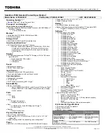
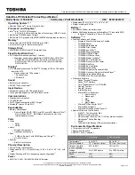
background image

Schematic  Diagrams

P PS8330B  B - 37

B.Schematic Diagrams

P PS8330B

Sheet 36 of 69

5

5

4

4

3

3

2

2

1

1

D

D

C

C

B

B

A

A

check IN_CA,1/13 

DESIGN NOTE:CFG0

Configuration pin for automatic EQ and
Aux interception; Internal pull down at
150Kohm,3.3V I/O

L: default, automatic EQ enable and Aux interception enable

H: automatic EQ disable and AUX interception enable

M: automatic EQ disable and AUX interception
disable,no pre-emphasis, 600mVpp swing

DESIGN NOTE:CFG1

Configuration pin for auto test and input offset
cancellation,3.3V IO, internal pull up at 150K

H: default, auto test disable and input offset cancellation
enable

L: auto test enable and input offset cancellation enable

M: auto test disable and input offset cancellation disable

DESIGN NOTE:PEQ

Programmalbe input equalization levels;internal pull
down at 150k ,3.3v I/O

L: default, LEQ, compensate channel loss up to 12dB at
HBR2

H: HEQ, compensate channel loss up to 15dB at HBR2

M:LLEQ, compensate channel loss up to 5dB at HBR2

DEFAULT:LOW

$XWRWHVWHQDEOH,QWHUQDOSXOOGRZQDWa.

,  3.3V  I/O.

   L: Auto test disable & input offset cancellation enable (default)
   H: Auto test enable & input offset cancellation enable
   M: Auto test disable & input offset cancellation disable

$XWRPDWLF(4GLVDEOH,QWHUQDOSXOOGRZQDWa.

,  3.3V  IO

   L: Automatic EQ enable (default)
   H: Automatic EQ disable

Programmable input equalization levels; Internal pull down at
~150K

,  3.3V  I/O.

   L: default, LEQ, compensate channel loss up to 11.5dB @ HBR2
   H: HEQ, compensate channel loss up to 14.5dB @ HBR2
   M: LLEQ, compensate channel loss up to 8.5dB @ HBR2

Port switching control or priority configuration; 
Internal pull down at ~150K

,  3.3V  I/O.

   L: Port1 is selected or with higher priority (default)
   H: Port2 is selected or with higher priority

Chip operational mode configuration; 
Internal pull down at ~150K

,   3.3V   I/O.

   L: Control switching mode (default)
   H: Automatic switching mode

3 Levels Input:
  L: Low
  H: High
  M: VDD33/2, connect both
pull-up and pull-down resistors

AUX interception disable for Port y (y = 1, 2). Internal pull down at ~150K

,  

9,2

   L: AUX interception enable, driver configuration is set by link training (default)
   H: AUX interception disable, driver output with fixed 800mV and 0dB
   M: AUX interception disable, driver output with fixed 400mV and 0dB

Hybrid DDC/AUX

Output swing adjustment for Port y (y = 1, 2). Internal pull down at ~150K

9,2

   L: default
   H: +20%
   M: -16.7%

PD PIN: 8330
HI ->DEFAULT
LOW->CHIP PWR DOWN

PD PIN: 8330
HI ->DEFAULT
LOW->CHIP PWR DOWN

PD PIN: 8338
L:default
H:Chip power down

PD PIN: 8338
L:(default)
H:Chip power down

CAD_SNK

PS8330B_CFG1

PS8330B_CFG0

PEQ

HPD_SRC

CAD_SRC

IN_DDC_SDA

IN_DDC_SCL

PS8330B_AUXp

PS8330B_AUXn

OUT2_AUXp_SCL

OUT2_AUXn_SDA

PS8330B_AUXn

PS8330B_AUXp

IN_DDC_SDA

IN_DDC_SCL

IN_DDC_SCL

CAD_SRC

IN_AUXn

IN_DDC_SDA
IN_DDC_SCL

DP_A1

DP_A#3

PS8330B_IN_D2n

IN_D2p

PI1

PI0

PSCFG0

PC11

PC20

PC21

PC10

PSPEQ

3.3VS

IN_D1p

PSPEQ

3.3VS

IN_CA_DET

PI0

PS8330B_IN_D3p

IN_D2n

DP_A#1

PS8330B_IN_D3n

IN_D3p

DP_A#2

IN_D3n

CAD_SRC

DP_A3

PI1

PSCFG0

DP_A2

PS8338B_SW

MUX_AUXP_DDC_SCL

MUX_AUXN_DDC_SDA

IN_AUXp

IN_AUXn

PC10

IN_AUXp

IN_CA_DET

GND

MUX_AUXP_DDC_SCL

MUX_AUXN_DDC_SDA

PC21

PC20

DP_A_HPD

PS8330B_IN_D0p

IN_D0p

PS8330B_IN_D0n

PS8330B_IN_D1p

IN_D0n

PS8330B_IN_D1n

DP_A0

PS8330B_IN_D2p

IN_D1n

DP_A#0

IN_DDC_SDA

PS8330B_IN_D0p

PS8330B_IN_D0n

IN0P_R

IN0N_R

PS8330B_IN_D1n

PS8330B_IN_D1p

IN1P_R

IN1N_R

PS8330B_IN_D2n

PS8330B_IN_D2p

IN2P_R

IN2N_R

PS8330B_IN_D3n

PS8330B_IN_D3p

IN3P_R

IN3N_R

HPD_SRC_R

HPD_SRC
OUT2_HPD

PC11

PS8330B_PCH

8338PD

PS8338B_PD

PS8330B_CFG1

PS8330B_CFG0

PEQ

8338PD

PS8338B_PD

3.3VS

3.3VS

3.3VS

3.3VS

3.3VS

3.3VS

3.3VS

3.3VS

3.3VS

3.3VS

3.3VS

3.3VS

3.3VS

3.3VS

3.3VS

3.3VS

3.3VS

3.3VS

3.3VS

3.3VS

3.3VS

3.3VS

NV3V3

NV3V3

NV3V3

3.3VS

3.3VS

3.3VS

3.3VS

OUT2_D0p

37

OUT2_D0n

37

OUT2_D1p

37

OUT2_D1n

37

OUT2_D2n

37

OUT2_D2p

37

OUT2_D3p

37

OUT2_D3n

37

DP_A0

12

DP_A#0

12

DP_A1

12

DP_A#1

12

DP_A2

12

DP_A#2

12

DP_A3

12

DP_A#3

12

DP_A_HPD

12

OUT2_AUXp_SCL

37

OUT2_AUXn_SDA

37

G_DPA_MODE

12

OUT2_HPD

37

OUT1_AUXp_SCL

12

OUT1_AUXn_SDA

12

MUX_0P

15

MUX_HPD

15

MUX_2P

15

MUX_1N

15

MUX_1P

15

MUX_0N

15

MUX_3N

15

MUX_3P

15

MUX_2N

15

MUX_AUXN_DDC_SDA

15

MUX_AUXP_DDC_SCL

15

3.3VS

7,8,9,10,11,14,15,16,17,18,19,20,21,24,25,26,27,28,30,31,32,33,34,38,41,42,43,44,46,47,49,51

PS8338B_SW

17

NV3V3

11,12,13,14,47

PS8330B_PCH

16

Title

Size

Document Number

R e v

Date:

Sheet

o f

6-71-P77F0-D02

2.0

[36] AR_PS8330B

A3

36

69

Monday, August 28, 2017

ᙔ!Ϻ!ႝ!တ!!DMFWP!DP/

SCHEMATIC1

Title

Size

Document Number

R e v

Date:

Sheet

o f

6-71-P77F0-D02

2.0

[36] AR_PS8330B

A3

36

69

Monday, August 28, 2017

ᙔ!Ϻ!ႝ!တ!!DMFWP!DP/

SCHEMATIC1

Title

Size

Document Number

R e v

Date:

Sheet

o f

6-71-P77F0-D02

2.0

[36] AR_PS8330B

A3

36

69

Monday, August 28, 2017

ᙔ!Ϻ!ႝ!တ!!DMFWP!DP/

SCHEMATIC1

R350

100K_04

C83

0.01u_16V_X7R_04

R68

*4.7K_04

R73

*4.7K_04

R529
4.7K_04

R537

*4.7K_04

R880

*0_04

Q53
2SK3018S3

G

D

S

R63

*4.7K_04

C82

0.1u_10V_X7R_04

R542

4.99K_1%_04

R540

100K_04

C71

0.1u_10V_X7R_04

C72

0.1u_10V_X7R_04

C75

0.1u_10V_X7R_04

C68

0.1u_10V_X7R_04

R69

*4.7K_04

R539

*4.7K_04

PS8330B

U26
PS8330B

VDD3

3

1

CEXT

2

I2

C_

ADDR

3

SCL

_

C

TL

PEQ

4

SDA_

CL

TCFG

0

5

VDD3

3

6

REXT

7

CAD_

SRC

8

HPD_

SRC

9

CAD_

SNK

10

HPD_

SNK

11

VDD3

3

12

OUT3n

13

OUT3p

14

NC

15

OUT2n

16

OOUT2p

17

GND

18

OUT1n

19

OUT1p

20

NC

21

OUT0n

22

OUT0p

23

GND

24

VDD3

3

36

RST

#

35

SDA_

DDC

34

SCL

_

DDC

33

VDD3

3

32

GND

31

AUX_

SRCp

30

AUX_

SRCn

29

AUX_

SNKp

28

AUX_

SNKn

27

PD#

26

VDD3

3

25

IN3n

48

IN3p

47

NC

46

IN2n

45

IN2p

44

NC

43

IN1n

42

IN1p

41

CFG1

40

IN0n

39

IN0p

38

NC

37

EPAD

49

Q43

AO3415

G

D

S

C336

0.1u_10V_X7R_04

C361

2.2u_6.3V_X5R_04

C569

0.1u_10V_X7R_04

Q44

AO3415

G

D

S

R544
4.7K_04

C66

2.2u_6.3V_X5R_04

R366

10K_04

R925

*100K_04

R368

*4.7K_04

C74

0.1u_10V_X7R_04

C576

0.1u_10V_X7R_04

R543

100K_04

C73

0.1u_10V_X7R_04

R567

100K_04

R924

*10K_04

R72

*4.7K_04

R351

100K_04

R384

*4.7K_04

C572

0.1u_10V_X7R_04

C556

0.1u_10V_X7R_04

R530
4.7K_04

R565

*0_04

R352

1M_04

R62

*4.7K_04

C86

0.01u_16V_X7R_04

R528

*4.7K_04

R74

*4.7K_04

R370

*4.7K_04

C575

0.1u_10V_X7R_04

C909

*0.1u_16V_Y5V_04

Q51

AO3415

G

D

S

C70

0.1u_10V_X7R_04

R367

*4.7K_04

R527

*4.7K_04

C573

0.1u_10V_X7R_04

R566

0_04

Q52

AO3415

G

D

S

R383

*4.7K_04

C87
0.1u_16V_X7R_04

R538

*4.7K_04

Q65
*2SK3018S3

G

D

S

C570

0.1u_10V_X7R_04

R353

4.99K_1%_04

R71

*4.7K_04

R546
4.7K_04

R923

*0_04

C360

0.01u_16V_X7R_04

Q7
2SK3018S3

G

D

S

R369

*4.7K_04

C574

0.1u_10V_X7R_04

R75

*4.7K_04

U7

PS8338B

PI1/SCL_CTL

1

I2C_CTL_EN

2

IN_HPD

3

IN_CA_DET

4

VDD33

5

IN_D0p

6

IN_D0n

7

PEQ

8

IN_D1p

9

IN_D1n

10

GND

11

IN_D2p

12

IN_D2n

13

PD

14

IN_D3p

15

IN_D3n

16

CEXT

17

SW

18

GND

19

REXT

20

VDD3

3

21

IN_

DDC_

SCL

22

IN_

DDC_

SDA

23

IN_

A

UXp

24

IN_

A

UXn

25

O

U

T

1_A

U

X

p_S

C

L

26

O

U

T

1_A

U

X

n_S

D

A

27

O

U

T

2_A

U

X

p_S

C

L

28

O

U

T

2_A

U

X

n_S

D

A

29

VDD3

3

30

OUT2_D3n

31

OUT2_D3p

32

OUT2_CA_DET

33

OUT2_D2n

34

OUT2_D2p

35

OUT2_D1n

36

OUT2_D1p

37

OUT2_HPD

38

OUT2_D0n

39

OUT2_D0p

40

OUT1_D3n

41

OUT1_D3p

42

OUT1_CA_DET

43

OUT1_D2n

44

OUT1_D2p

45

OUT1_D1n

46

OUT1_D1p

47

OUT1_HPD

48

OUT1_D0n

49

OUT1_D0p

50

VDD3

3

51

GND

52

PC2

1

53

PC2

0

54

PC1

1

55

PC1

0

56

VDD3

3

57

CF

G1

58

CF

G0

59

PI0

/SDA_

CTL

60

EPAD

61

R541

100K_04

C65

0.1u_10V_X7R_04

R70

*4.7K_04

C359

2.2u_6.3V_X5R_04

R531
4.7K_04

C571

0.1u_10V_X7R_04

R545
4.7K_04

C67

0.1u_10V_X7R_04

C567

0.1u_10V_X7R_04

C69

0.1u_10V_X7R_04

C81

0.1u_10V_X7R_04

Summary of Contents for P775TM

Page 1: ...P775TM G P775TM1 G ...

Page 2: ......

Page 3: ...Preface I Preface Notebook Computer P775TM G P775TM1 G Service Manual ...

Page 4: ...le or in part be reproduced translated transmitted or reduced to any machine readable form without prior consent from the vendor manufacturer or creators of this publica tion except for copies kept by the user for backup purposes Brand and product names mentioned in this publication may or may not be copyrights and or registered trademarks of their respective companies They are mentioned for ident...

Page 5: ...ing and or upgrading components of the P775TM G P775TM1 G series notebook PC The following information is included Chapter 1 Introduction provides general information about the location of system elements and their specifications Chapter 2 Disassembly provides step by step instructions for disassembling parts and subsystems and how to upgrade elements of the system Appendix A Part Lists Appendix B...

Page 6: ...g a telephone other than a cordless type during an electrical storm There may be a remote risk of elec trical shock from lightning 3 Do not use the telephone to report a gas leak in the vicinity of the leak 4 Use only the power cord and batteries indicated in this manual Do not dispose of batteries in a fire They may explode Check with local codes for possible special disposal instructions 5 This ...

Page 7: ... down properly and don t forget to save your work Remember to periodically save your data as data may be lost if the battery is depleted Do not expose the computer to any shock or vibration Do not place it on an unstable surface Do not place anything heavy on the computer Do not expose it to excessive heat or direct sunlight Do not leave it in a place where foreign matter or mois ture may affect t...

Page 8: ...be sure to disconnect it by the plug head not by its wire Make sure the socket and any extension cord s you use can support the total current load of all the connected devices Before cleaning the computer make sure it is disconnected from any external power supplies Use only approved brands of peripherals Unplug the power cord before attaching peripheral devices Do not plug in the power cord if yo...

Page 9: ...ur hands or metal objects Battery Guidelines The following can also apply to any backup batteries you may have If you do not use the battery for an extended period then remove the battery from the computer for storage Before removing the battery for storage charge it to 60 70 Check stored batteries at least every 3 months and charge them to 60 70 Battery Disposal The product that you have purchase...

Page 10: ...ollowing procedure as to safeguard the computer during shipping the battery will be locked to not power the system until first connected to the AC DC adapter and initially set up as below Attach the AC DC adapter cord to the DC In jack at the rear of the computer then plug the AC power cord into an outlet and connect the AC power cord to the AC DC adapter and leave it there for 6 seconds or longer...

Page 11: ...2 10 Removing and Installing the Processor 2 12 Removing the System Memory RAM from Under the Keyboard 2 15 Removing the Wireless LAN Module 2 17 Wireless LAN Combo Module Cables 2 18 Removing the WiGig Module 2 19 Removing the M 2 SSD Module 2 20 Removing and Installing the Video Card 2 22 Part Lists A 1 Part List Illustration Location A 2 Top A 3 Bottom A 4 LCD LG AU A 5 LCD AU A 6 MB A 7 HDD A ...

Page 12: ... 1 2V 0 6VS VCCPLL_OC B 45 VDD3 VDD5 B 46 5V 5VS 3V 3 3VS 3 3VA B 47 5VS_2 2 5V NV3V3 3 3V_ON 5V_RUN B 48 Fan CPU VGA Power B 49 VCore B 50 VCore Output Stage B 51 VCCSA VCCGT B 52 Power Charger DC In B 53 P750DM HDD Board B 54 P750DM Power LED Board B 55 P750DM Click Board B 56 P750DM Audio Board B 57 P750DM Audio ESS DAC B 58 P750DM Audio HP AMP B 59 P750DM Audio Board B 60 P775DM Audio Board B ...

Page 13: ...al is shipped with the computer Operating systems e g Windows 10 etc have their own manuals as do application software e g word processing and database programs If you have questions about those programs you should consult those manuals The P775TM G P775TM1 G series notebook is designed to be upgradeable See Disassembly on page 2 1 for a detailed description of the upgrade procedures for each spec...

Page 14: ... ROM Pointing Device Built In Secure Pad with Microsoft PTP Multi Gesture Scrolling Functionality Keyboard Full Color Illuminated Full size Winkey Keyboard with numeric keypad and anti ghost keys Video Adapter Options NVIDIA GeForce GTX 1060 PCIe Video Card 6GB GDDR5 Video RAM on board Supports GPU Overclocking NVIDIA GeForce GTX 1070 GTX 1080 PCIe Video Card for P775TM1 G only 8GB GDDR5 Video RAM...

Page 15: ...Atheros Killer Wireless AC 1535 Wireless LAN 802 11ac Bluetooth 4 1 Factory Option Qualcomm Wireless LAN 802 11ac ad Bluetooth 4 1 M 2 Slots Slot 1 for Combo WLAN and Bluetooth Module Slot 2 for SATA or PCIe Gen3 x4 SSD Slot 3 for SATA or PCIe Gen3 x4 SSD Card Reader Embedded Multi In 1 Push Push Card Reader MMC MultiMedia Card RS MMC SD Secure Digital Mini SD SDHC SDXC up to UHS II Features Suppo...

Page 16: ...1 Introduction External Locator Top View with LCD Panel Open Figure 1 Top View 1 PC Camera 2 PC Camera LED 3 Built In Microphone 4 LCD 5 Speakers 6 Power Button 7 LED Lock Indicators 8 Keyboard 9 TouchPad and Buttons 10 Fingerprint Reader 2 1 8 9 7 6 5 4 5 3 10 3 7 ...

Page 17: ...uction External Locator Front Right side Views Figure 2 Front Views 1 LED Power Indicators Figure 3 Right Side Views 1 Line In Jack 2 Microphone Jack 3 Line Out Jack 4 Headphone and S PDIF Combo Jack 5 USB 3 0 3 1 Port 6 Security Lock Slot 1 Front Right 1 2 3 4 5 6 5 ...

Page 18: ...iew Figure 4 Left Side View 1 RJ 45 LAN Jack 2 USB 3 1 Thunderbolt Combo Port 3 USB 3 1 Port 4 USB 3 0 3 1 Port 5 Powered USB 3 1 Port 6 Multi in 1 Card Reader 4 6 1 3 Left 2 5 Figure 5 Rear View 1 Vent Fan Intake 2 HDMI Out Port 3 Mini Display Port 1 4 Mini Display Port 2 5 DC In Jack Rear 4 1 2 3 1 5 ...

Page 19: ...on External Locator Bottom View Figure 6 Bottom View 1 Vent 2 Component Bay Cover 3 Battery 4 Sub Woofer 5 HDD Bay Overheating To prevent your com puter from overheating make sure nothing blocks the vent fan in takes while the com puter is in use 3 2 5 1 1 1 4 ...

Page 20: ...Introduction 1 8 Mainboard Overview Top Key Parts 1 Introduction Mainboard Overview Top Key Parts Figure 7 Mainboard Top Key Parts 1 Memory Slots DDR4 SO DIMM 2 Platform Controller Hub 1 2 ...

Page 21: ... Key Parts 1 9 1 Introduction Mainboard Overview Bottom Key Parts Figure 8 Mainboard Bottom Key Parts 1 KBC ITE IT8587 2 VGA Card Connector 3 CPU Socket no CPU installed 4 Memory Slots DDR4 SO DIMM Primary 5 Hard Disk Connector 5 2 1 4 3 1 ...

Page 22: ...olt Combo Port 3 USB 3 1 Port 4 USB 3 0 3 1 Port 5 Multi in 1 Card Reader 6 KB LED Connector 7 WLAN Card Connector 8 Fingerprint Connector 9 TP FFC Cable Connector 10 Panel Cable Connector 11 Keyboard Cable Connector 12 Battery Connector 13 Line In Jack 14 Microphone Jack 15 Line Out Jack 16 Headphone and S PDIF Combo Jack 1 4 5 6 7 8 14 9 12 13 15 2 3 10 11 11 4 16 4 4 ...

Page 23: ...1 1 Introduction Mainboard Overview Bottom Connectors Figure 10 Mainboard Bottom Connectors 1 HDMI Out Port 2 Display Port 3 DC In Jack 4 VGA Fan Cable Connector 5 3G SSD Connector 6 CMOS Battery 7 SSD Connector 8 CPU Fan Cable Connector 1 2 3 4 2 6 5 7 8 ...

Page 24: ...Introduction 1 12 1 Introduction ...

Page 25: ...disassembly process easier each section may have a box in the page margin Information contained under the figure will give a synopsis of the sequence of procedures involved in the disassembly procedure A box with a lists the relevant parts you will have after the disassembly process is complete Note The parts listed will be for the dis assembly procedure listed ONLY and not any previous disassembl...

Page 26: ...acing the connection make sure the connector is oriented in the same way The pin1 side is usually not indicated Pressure sockets for multi wire connectors To release this connector type grasp it at its head and gently rock it from side to side as you pull it out Do not pull on the wires themselves When replacing the connection do not try to force it The socket only fits one way Pressure sockets fo...

Page 27: ...the computer When handling a printed circuit board do not use gloves or other materials which allow static electricity buildup We suggest that you use an anti static wrist strap instead 8 Beware of corrosion As you perform your job avoid touching any connector leads Even the cleanest hands produce oils which can attract corrosive elements 9 Keep your work environment clean Tobacco smoke dust or ot...

Page 28: ...2 10 3 Remove the processor page 2 12 4 Install the processor page 2 14 To remove the System Memory under the Keyboard 1 Remove the battery page 2 5 2 Remove the processor page 2 12 3 Remove the keyboard page 2 15 4 Remove the system memory page 2 16 To remove the WLAN Module 1 Remove the battery page 2 5 2 Remove the processor page 2 12 3 Remove the keyboard page 2 10 4 Remove the wireless LAN pa...

Page 29: ...Figure 1a 3 Slide the latch in the direction of the arrow and hold it in place Figure 1a 4 Lift the battery in the direction of the arrow 5 Lift the battery out of the compartment Figure 1c 4 Battery 1 2 3 6 4 a b 1 2 4 3 c Figure 1 Battery Removal a Slide the latch and hold in place b Lift the battery up toward the direction of the arrow c Lift the battery out ...

Page 30: ...e 2 5 2 Locate the hard disk bay cover and remove screws Figure 2a 3 Remove the hard disk bay cover by sliding the cover at point Figure 2b Figure 2 HDD Assembly Removal a Locate the HDD bay cover and remove the screws b Remove the hard disk bay cover by sliding the cover at point 3 2 Screws 1 2 3 HDD System Warning New HDD s are blank Before you begin make sure You have backed up any data you wan...

Page 31: ...m the hard disk Figure 3f 8 Reverse the process to install a new hard disk do not forget to replace all the screws and covers 6 4 5 6 6 7 8 9 10 11 16 17 18 19 c 4 f 10 9 d 18 6 HDD 2 HDD 1 7 19 13 12 14 5 8 11 15 16 17 e 4 HDD Bay Cover 7 HDD 1 Assembly 10 HDD 2 Assembly 17 Adhesive Cover 18 HDD Bracket 19 HDD 8 Screws Figure 3 HDD Assembly Removal cont d c Remove the HDD bay cover d Remove the s...

Page 32: ...red on the following pages are all 9 5mm H hard disk drives In some cases 7mm H hard disk drives will be installed Figure 4 Foam Rubber Insert for 7mm H HDDs If you are replacing a 9 5mm H HDD with a 7mm H HDD then insert the foam rubber insert If you are replacing a 7mm H HDD with a 9 5mm H HDD then remove the foam rub ber insert HDD 2 HDD 1 ...

Page 33: ...crew from the SSD Figure 5a 3 The M 2 SSD module will pop up Figure 5b 4 Lift the M 2 SSD module up and off the computer Figure 5c 5 Reverse the process to install a new SSD make sure that the hexagonal screw is in the correct location depending upon the size of the module 2 M 2 SSD Module 1 Screw Figure 5 M 2 SSD Module Removal a Remove the screws b The module will pop up c Lift the module out 1 ...

Page 34: ...econdary memory sockets are located under the keyboard not user upgradable If you are installing only two RAM modules then they should be installed in the primary memory sockets under the component bay cover Note that the RAM located under the keyboard is not user upgradable Memory Upgrade Process 1 Turn off the computer and turn it over remove the battery page 2 5 2 Remove screws 3 Slide the bott...

Page 35: ...ORCE the module it should fit without much pressure 10 Press the module in and down towards the mainboard until the slot levers click into place to secure the module 11 Replace the bay cover and screws 12 Restart the computer to allow the BIOS to register the new memory configuration as it starts up 6 6 7 Figure 7 RAM Module Removal cont d c Lift the component bay cover off the computer case The m...

Page 36: ...10 2 Remove screws from the heat sink unit in the order indicated on the label i e screw first through to screw last Figure 8a 3 Carefully it may be hot remove the heat sink unit Figure 8b 1 4 4 1 5 Figure 8 Processor Removal Procedure a Remove the screws in the correct order b Carefully remove the heat sink unit 5 Heat Sink Unit 4 Screws a b Note Loosen the screws in the reverse order 4 3 2 1 as ...

Page 37: ... 9d 7 See page 2 14 for information on inserting a new CPU 8 When re inserting the CPU pay careful attention to the pin alignment it will fit only one way DO NOT FORCE IT 11 11 12 A Figure 9 Processor Removal cont d c Move the latch and bracket fully in the direc tion indicated to unlock the CPU d Lift the CPU out of the socket Caution The heat sink and CPU area in general contains parts which are...

Page 38: ... unit if it is a new unit 5 Insert the heat sink unit as indicated in Figure 10c 6 Tighten the CPU heat sink screws in the order the order as indicated on the label and Figure 10d 7 Replace the CPU fan component bay cover and tighten the screws page 2 12 A B C D E F 1 4 b c d C a E F 1 4 2 Note Tighten the screws in the order 1 2 3 4 as indicated 3 A B D C Figure 10 Processor Installation a Insert...

Page 39: ...s under the component bay cover Memory Upgrade Process 1 Turn off the computer and turn it over remove the battery page 2 5 2 Remove screws and the component bay cover Figure 11a and CPU heatsink page 2 12 3 Remove screws from the bottom of the computer Figure 11b 4 Open it up with the LCD on a flat surface before pressing at point to release the keyboard module use an eject stick to do this with ...

Page 40: ... fit one way Make sure the module is seated as far into the slot as it will go DO NOT FORCE the module it should fit without much pressure 13 Press the module in and down towards the mainboard until the slot levers click into place to secure the module 14 Replace the bay cover and screws 15 Restart the computer to allow the BIOS to register the new memory configuration as it starts up 12 13 15 13 ...

Page 41: ...e 13a 3 Carefully disconnect cables then remove screw from the module socket Figure 13b 4 The Wireless LAN module will pop up Figure 13c 5 Lift the Wireless LAN module Figure 13d up and off the computer Figure 13 Wireless LAN Module Removal a The Wireless LAN mod ule will be visible at point under the keyboard b Disconnect the cables and remove the screw c The WLAN module will pop up d Lift the WL...

Page 42: ... are not labelled The cables covers each cable will have either a black or transparent cable cover are color coded for iden tification as outlined in the table below Cable 1 is usually connected to antenna 1 Main on the module and cable 2 to antenna 2 Aux Module Type Antenna Type Cable Color Cable Cover Type WLAN WLAN Bluetooth Combo WM 1 Black Transparent WM 2 Black White WiGig WG 1 Blue Black ...

Page 43: ...eyboard Figure 13a 3 Carefully disconnect cables then remove screw from the module socket Figure 13b 4 The module will pop up Figure 13c 5 Lift the module Figure 13d up and off the computer Figure 14 WiGig Module Removal a The module will be visi ble at point under the keyboard b Disconnect the cables and remove the screw c The module will pop up d Lift the module out 1 1 2 4 5 6 6 b a d 2 3 6 c 4...

Page 44: ...remove the screw from the module Figure 15b 4 The M 2 SATA module will pop up Figure 15c 5 Lift the M 2 SATA module up and off the computer Figure 15d 6 Reverse the process to install a new SSD make sure that the hexagonal screw is in the correct location Figure 15 M 2 SSD Module Removal a Locate the module b Remove the screw c The module will pop up d Lift the module up off the socket 1 2 6 3 6 3...

Page 45: ...b Insert the module c Tighten the screw 2 3 4 a 4 2 b 1 c 3 Thermal Pad Make sure you place the thermal pad s adhe sive side down onto the computer surface as illustrated The usage of the thermal pad will depend upon the thickness of the module being used If you are using the thinner module then apply the whole thermal pad provided on the computer If you are using the thicker module sepa rate the ...

Page 46: ...e 17c 5 Remove the video card Figure 17d 6 Heat Sink Units 10 Video Card 5 Screws Caution The heat sink and video card area in general contains parts which are subject to high tempera tures Allow the area time to cool before re moving these parts Figure 17 Video Card Removal Procedure a Remove the screws in the correct order b Carefully remove the heat sink units c Remove the video card screws The...

Page 47: ...will go DO NOT FORCE the card it should fit without much pressure 7 Connect the cable and secure the card with screws Figure 17 on page 2 22 8 Apply the whole tube of the thermal grease to the center of the main VGA chip as shown Figure 18h 9 Place the heat sink back on the card and secure the screws in the order indicated in Figure 17 on page 2 22 10 Reinsert the component bay cover and secure wi...

Page 48: ...Disassembly 2 24 2 Disassembly ...

Page 49: ...art numbers Your organization may use a different system so be sure to cross check any relevant documentation Note Some assemblies may have parts in common especially screws However the part lists DO NOT indicate the total number of duplicated parts used Note Be sure to check any update notices The parts shown in these illustrations are appropriate for the system at the time of publication Over th...

Page 50: ...ustration Location The following table indicates where to find the appropriate part list illustration Table A 1 Part List Illustration Location Parts Top page A 3 Bottom page A 4 LCD LG AU page A 5 LCD AU page A 6 MB page A 7 HDD page A 8 VGA G1 G3 page A 9 VGA G2 page A 10 ...

Page 51: ...Part Lists Top A 3 A Part Lists Top Figure A 1 Top ...

Page 52: ...Part Lists A 4 Bottom A Part Lists Bottom Figure A 2 Bottom ...

Page 53: ...Part Lists LCD LG AU A 5 A Part Lists LCD LG AU Figure A 3 LCD LG AU ...

Page 54: ...Part Lists A 6 LCD AU A Part Lists LCD AU Figure A 4 LCD AU ...

Page 55: ...Part Lists MB A 7 A Part Lists MB Figure A 5 MB ...

Page 56: ...Part Lists A 8 HDD A Part Lists HDD Figure A 6 HDD ...

Page 57: ...Part Lists VGA G1 G3 A 9 A Part Lists VGA G1 G3 Figure A 7 VGA G1 G3 ...

Page 58: ...Part Lists A 10 VGA G2 A Part Lists VGA G2 Figure A 8 VGA G2 ...

Page 59: ...Inverter CRT Page B 12 LAN E2500 Page B 36 P750DM Audio Board Page B 60 Display Port A Page B 13 PS8338B PS8330B Page B 37 P775DM Audio Board Page B 61 Display Port B Page B 14 TBT Page B 38 P775DM Audio ESS DAC Page B 62 HDMI Page B 15 Power Page B 39 P775DM Audio HP AMP Page B 63 MXM PCI E Page B 16 TPS65982 Page B 40 P775DM Audio Board Page B 64 Lynix Point 1 7 Page B 17 TPS65982 Page B 41 P750...

Page 60: ...TEM SMBUS ITE 8587A 512KB ROM ITE 8587A Azalia Codec USB 2 0 DMI 4 Qualcomm SATA I II III 6 0Gb s SHEET 24 FingerPrint 12 MHz SHEET 54 FINGER PRINTER ON CLICK BOARD 2333 MHz DDR4 1 2V DDR IV SHEET 7 8 9 10 SO DIMM 4 PCIE 16 Optional USB2 USB 3 0 5 Gbps SOCKET NGFF PCIE SHEET 25 WLAN BT USB11 E2500 Charging SHEET 56 63 AUDIO BOARD A KEY SHEET 35 SHEET 40 SOCKET 3IN1 RJ 45 M KEY NGFF PCIE SOCKET SHE...

Page 61: ...TXN 3 AF3 DMI_TXP 3 AF2 DMI_TXN 2 AE1 DMI_TXP 2 AE2 DMI_TXP 1 AD3 DMI_TXN 1 AD2 DMI_TXN 0 AC1 DMI_TXP 0 AC2 DMI_RXP 3 AC4 DMI_RXN 3 AC5 DMI_RXN 2 AB3 DMI_RXP 2 AB4 DMI_RXP 1 AA4 DMI_RXN 1 AA5 DMI_RXP 0 Y3 DMI_RXN 0 Y4 PEG_RCOMP L7 PEG_RXP 15 U5 PEG_RXP 14 T6 PEG_RXN 15 U4 PEG_RXP 8 K6 PEG_RXN 7 J4 PEG_RXP 7 J5 PEG_RXN 0 B7 PEG_RXP 1 C7 PEG_RXN 1 C6 PEG_RXP 4 F6 PEG_RXP 5 G5 PEG_RXP 6 H6 PEG_RXP 10...

Page 62: ...WP DP SCHEMATIC1 Title Size Document Number Rev Date Sheet o f 6 71 P77F0 D02 2 0 03 Processor 2 5 CLK MISC DIS A3 3 69 Wednesday October 25 2017 ᙔ Ϻ ႝ တ DMFWP DP SCHEMATIC1 Title Size Document Number Rev Date Sheet o f 6 71 P77F0 D02 2 0 03 Processor 2 5 CLK MISC DIS A3 3 69 Wednesday October 25 2017 ᙔ Ϻ ႝ တ DMFWP DP SCHEMATIC1 R579 2 74K_1 _04 R91 20mil_04 R572 1K_1 _04 R549 51_04 R64 100K_04 R5...

Page 63: ...R1_DQ 63 AF6 DDR1_ECC 0 AR25 DDR1_ECC 1 AR26 DDR1_ECC 2 AM26 DDR1_ECC 3 AM25 DDR1_ECC 5 AP25 DDR1_ECC 4 AP26 DDR1_ECC 7 AL26 DDR1_ECC 6 AL25 DDR1_CKN 0 AM21 DDR1_CKP 0 AM20 DDR1_CKP 1 AP22 DDR1_CKN 1 AP21 DDR1_CKP 2 AN20 DDR1_CKN 2 AN21 DDR1_CKP 3 AP19 DDR1_CKN 3 AP20 DDR1_CKE 0 AY29 DDR1_CKE 1 AV29 DDR1_CKE 2 AW29 DDR1_CS 0 AP17 DDR1_CKE 3 AU29 DDR1_CS 1 AN15 DDR1_ODT 3 AL15 DDR1_CAS DDR1_CAB 1 D...

Page 64: ...CCOPC AJ28 VCCIO AK24 VCCOPC_SENSE AK21 VCCEOPIO_SENSE AJ24 VSSOPC_EOPIO_SENSE AK22 VCCSA AB6 VCCSA AA7 VDDQ AT21 VDDQ AU13 VDDQ AU15 VDDQ AU19 VDDQ AV17 VDDQ AT18 VCCSA AB7 VCCSA AB8 VCCSA AC7 VCCSA AC8 VCCSA N7 VCCSA P7 VCCSA R7 VCCSA T7 VCCSA U7 VCCSA Y6 VCCSA Y8 VCCSA W7 VCCSA V7 VCCIO AK11 VCCIO M8 VCCIO P8 VCCIO U8 VCCIO W8 VCCST V5 VCCPLL V4 VCCSA AA6 VCCSA Y7 C579 22u_6 3V_X5R_08 C582 22u_...

Page 65: ...VSS AM35 VSS AM36 VSS AM37 VSS AM38 VSS AM39 VSS AM40 VSS AM5 VSS AN1 VSS AN10 VSS AN11 VSS AN14 VSS AN16 VSS AN19 VSS AN22 VSS AN23 VSS AN24 VSS AN27 VSS AN30 VSS AN36 VSS AN4 VSS AN5 VSS AN6 VSS AN7 VSS AN8 VSS AN9 VSS AP11 VSS AP14 VSS AP24 VSS AP27 VSS AP30 VSS AP36 VSS AP37 VSS AP40 VSS AP5 VSS AR1 VSS AR11 VSS AR14 VSS AR16 VSS AR17 VSS AR18 VSS AR19 VSS AR2 VSS AR20 VSS AR21 VSS AD37 VSS AD...

Page 66: ...60 VDD17 159 VDD16 154 VDD15 153 VDD14 148 VDD13 147 VDD12 142 VDD11 141 VDD10 136 VDD9 135 VDD8 130 VDD7 129 VDD6 124 VDD5 123 VDD4 118 VDD3 117 VDD2 112 VDD1 111 VSS 251 VSS 247 VSS 243 VSS 239 VSS 235 VSS 231 VSS 227 VSS 223 VSS 217 VSS 213 VSS 209 VSS 205 VSS 201 VSS 197 VSS 193 VSS 189 VSS 185 VSS 181 VSS 175 VSS 171 VSS 167 VSS 107 VSS 103 VSS 99 VSS 93 VSS 89 VSS 85 VSS 81 VSS 77 VSS 73 VSS...

Page 67: ...1u_6 3V_X5R_04 C686 10u_6 3V_X5R_06 C231 1u_6 3V_X5R_04 C225 1u_6 3V_X5R_04 C671 10u_6 3V_X5R_06 C221 1u_6 3V_X5R_04 JDIMM2A D4AS0 26001 1P40 CK0_T 137 CK0_C 139 CK1_T 138 CK1_C 140 CKE0 109 CKE1 110 S0 149 S1 157 ODT0 155 ODT1 161 BG0 115 BG1 113 BA0 150 BA1 145 A0 144 A1 133 A2 132 A3 131 A4 128 A5 126 A6 127 A7 122 A8 125 A9 121 A10_AP 146 A11 120 A12 119 A13 158 A14_WE 151 A15_CAS 156 A16_RAS ...

Page 68: ...98 10u_6 3V_X5R_06 C651 0 1u_16V_X7R_04 C828 0 1u_10V_X7R_04 C703 10u_6 3V_X5R_06 C220 1u_6 3V_X5R_04 C815 0 1u_16V_X7R_04 C701 1u_6 3V_X5R_04 C827 1u_6 3V_X5R_04 C831 1u_6 3V_X5R_04 C176 10u_6 3V_X5R_06 C702 10u_6 3V_X5R_06 R860 2_1 _04 R861 24 9_1 _04 R859 0_04 C850 0 022u_16V_X7R_04 C826 1u_6 3V_X5R_04 C652 10u_6 3V_X5R_06 C820 2 2u_10V_X5R_04 C187 10u_6 3V_X5R_06 C774 10u_6 3V_X5R_06 C222 1u_6...

Page 69: ...V_X5R_04 C772 10u_6 3V_X5R_06 C314 1u_6 3V_X5R_04 C297 10u_6 3V_X5R_06 JDIMM4B D4AR0 26001 1P40 VDD19 163 VDD18 160 VDD17 159 VDD16 154 VDD15 153 VDD14 148 VDD13 147 VDD12 142 VDD11 141 VDD10 136 VDD9 135 VDD8 130 VDD7 129 VDD6 124 VDD5 123 VDD4 118 VDD3 117 VDD2 112 VDD1 111 VSS 251 VSS 247 VSS 243 VSS 239 VSS 235 VSS 231 VSS 227 VSS 223 VSS 217 VSS 213 VSS 209 VSS 205 VSS 201 VSS 197 VSS 193 VSS...

Page 70: ...တ DMFWP DP SCHEMATIC1 Title Size Document Number Rev Date Sheet o f 6 71 P77F0 D02 2 0 11 PANEL INVERTER CRT A3 11 69 Wednesday October 25 2017 ᙔ Ϻ ႝ တ DMFWP DP SCHEMATIC1 R562 100K_04 C48 0 1u_10V_X7R_04 R53 1K_04 C562 0 1u_50V_Y5V_06 R563 150K_1 _04 R564 100K_04 R56 100K_04 S D G Q50A MTDK5S6R 2 6 1 C916 22u_6 3V_X5R_06 Q49B MTS3572G6 S1 2 D1 6 G1 1 C50 0 1u_10V_X7R_04 U8A 74LVC08APW 1 2 3 14 7 ...

Page 71: ...Monday August 28 2017 ᙔ Ϻ ႝ တ DMFWP DP Title Size Document Number Rev Date Sheet o f 6 71 P77F0 D02 2 0 12 DISPLAY PORTA A3 12 69 Monday August 28 2017 ᙔ Ϻ ႝ တ DMFWP DP Title Size Document Number Rev Date Sheet o f 6 71 P77F0 D02 2 0 12 DISPLAY PORTA A3 12 69 Monday August 28 2017 ᙔ Ϻ ႝ တ DMFWP DP R31 0_04 L27 HCB1005KF 121T20 C19 0 1u_10V_X7R_04 D5 DT1140 04LP 7 5 1 2 3 4 10 9 8 7 6 R36 0_04 LP7 ...

Page 72: ...69 Monday August 28 2017 ᙔ Ϻ ႝ တ DMFWP DP Title Size Document Number Rev Date Sheet o f 6 71 P77F0 D02 2 0 13 DISPLAY PORTB A3 13 69 Monday August 28 2017 ᙔ Ϻ ႝ တ DMFWP DP R14 1K_04 S D G Q40A MTDK5S6R 2 6 1 S D G Q39A MTDK5S6R 2 6 1 R26 0_04 C A A D40 BAT54CW lision 1 2 3 LP2 DVI2012F2SF 900T05_08 1 4 2 3 C7 0 1u_10V_X7R_04 D4 DT1140 04LP 7 5 1 2 3 4 10 9 8 7 6 D1 BAV99 RECTIFIER A C AC R23 0_04 ...

Page 73: ...LK 15 HDMI_HPD 15 NV3V3 11 12 13 36 47 Title Size Document Number Rev Date Sheet o f 6 71 P77F0 D02 2 0 14 HDMI A3 14 69 Monday August 28 2017 ᙔ Ϻ ႝ တ DMFWP DP SCHEMATIC1 Title Size Document Number Rev Date Sheet o f 6 71 P77F0 D02 2 0 14 HDMI A3 14 69 Monday August 28 2017 ᙔ Ϻ ႝ တ DMFWP DP SCHEMATIC1 Title Size Document Number Rev Date Sheet o f 6 71 P77F0 D02 2 0 14 HDMI A3 14 69 Monday August 2...

Page 74: ...2 3 4 5 6 7 8 9 C559 10u_25V_X5R_08 R491 2 2K_04 R10 0_04 R533 20K_06 H32 H6_0B4_0D4_0 U37 74AHC1G32GW 4 5 3 1 2 C906 22u_25V_X5R_12 R9 0_04 R522 10K_04 R2 0_04 R504 10K_04 PC199 EEEFZ1E101P 1 2 R502 0_04 R500 0_04 Q48 2SK3018S3 G D S R519 100K_04 PJ49 OPEN 3mm 1 2 R20 0_04 R512 0_04 R526 10mil_short C483 10u_6 3V_X5R_06 PC200 EEEFZ1E101P 1 2 R492 2 2K_04 R600 0_04 Q46 MEP4435Q8 4 6 2 5 7 3 1 8 S ...

Page 75: ... 2017 ᙔ Ϻ ႝ တ DMFWP DP SCHEMATIC1 Title Size Document Number Rev Date Sheet o f 6 71 P77F0 D02 2 0 16 Lynx 1 7 SPI GPP A3 16 69 Wednesday October 25 2017 ᙔ Ϻ ႝ တ DMFWP DP SCHEMATIC1 R930 10K_04 R196 33_04 R692 33_04 R641 1K_04 S D G Q55B MTDK5S6R 5 3 4 R679 8 2K_04 J_80DEBUG2 85204 04001 1 2 3 4 R637 1K_04 R697 10mil_short R710 10K_04 R703 10K_04 R700 1K_04 R185 33_04 R693 33_04 R868 10K_04 R643 1...

Page 76: ...6 1 C316 0 1u_10V_X7R_04 R172 0_04 C184 0 22u_10V_X5R_04 R240 10K_04 R241 100K_04 C181 0 22u_10V_X5R_04 R154 10K_04 U7E1 3 OF 13 REV 0 7 U17C KBL_PCH_H PECI AK4 PM_DOWN AH2 PM_SYNC AH3 PCIE9_RXN SATA0A_RXN G31 PCIE20_TXP SATA7_TXP J44 PCIE16_TXN SATA3_TXN B39 PLTRST_PROC AK3 PCIE17_TXP SATA4_TXP F45 PCIE13_RXP SATA0B_RXP E35 CL_RST AW2 GPP_F19 EDP_VDDEN AC42 GPP_F12 SDATAOUT1 AE44 GPP_F11 SLOAD AH...

Page 77: ...LK 16 28 34 44 DDR_VOLTAGE_SEL 44 SUSC 31 44 46 47 SUS_CLK 25 Title Size Document Number Rev Date Sheet o f 6 71 P77F0 D02 2 0 18 Lynx 3 7 HDA SMB JTAG GPI A3 18 69 Wednesday October 25 2017 ᙔ Ϻ ႝ တ DMFWP DP SCHEMATIC1 Title Size Document Number Rev Date Sheet o f 6 71 P77F0 D02 2 0 18 Lynx 3 7 HDA SMB JTAG GPI A3 18 69 Wednesday October 25 2017 ᙔ Ϻ ႝ တ DMFWP DP SCHEMATIC1 Title Size Document Numb...

Page 78: ...HEMATIC1 Title Size Document Number Rev Date Sheet o f 6 71 P77F0 D02 2 0 19 Lynx 4 7 CLK REQ GPP A3 19 69 Wednesday October 25 2017 ᙔ Ϻ ႝ တ DMFWP DP SCHEMATIC1 R254 2 7K_1 _04 R669 10K_04 U7E1 5 OF 13 REV 0 7 U17E KBL_PCH_H GPP_I10 DDPD_CTRLDATA AY2 GPP_I2 DDPD_HPD2 AP8 GPP_I6 DDPB_CTRLDATA AV7 GPP_G20 Y35 GPP_I9 DDPD_CTRLCLK AY1 GPP_G21 AC30 GPP_F22 AB45 GPP_G22 R45 GPP_F23 AE39 GPP_I7 DDPC_CTRL...

Page 79: ...Date Sheet o f 6 71 P77F0 D02 2 0 20 Lynx 5 7 DMI PCIe USB A3 20 69 Monday August 28 2017 ᙔ Ϻ ႝ တ DMFWP DP SCHEMATIC1 R713 10K_04 C698 0 1u_10V_X7R_04 U7E1 2 OF 13 REV 0 7 U17B KBL_PCH_H PCIE_RCOMPN B10 PCIE_RCOMPP C10 USB2_COMP AG3 USB2_ID AG2 USB2_VBUSSENSE AE10 USB2N_1 AH5 USB2N_10 AK8 USB2N_11 W2 USB2N_12 AD3 USB2N_13 V3 USB2N_14 AK11 USB2N_2 AE5 USB2N_3 AH8 USB2N_4 AE2 USB2N_5 AC2 USB2N_6 AF2...

Page 80: ...er 25 2017 ᙔ Ϻ ႝ တ DMFWP DP SCHEMATIC1 Title Size Document Number Rev Date Sheet o f 6 71 P77F0 D02 2 0 21 Lynx 6 7 POWER A3 21 69 Wednesday October 25 2017 ᙔ Ϻ ႝ တ DMFWP DP SCHEMATIC1 Title Size Document Number Rev Date Sheet o f 6 71 P77F0 D02 2 0 21 Lynx 6 7 POWER A3 21 69 Wednesday October 25 2017 ᙔ Ϻ ႝ တ DMFWP DP SCHEMATIC1 C696 1u_6 3V_X5R_04 R279 1K_04 R178 15mil_short_06 C272 1u_6 3V_X5R_0...

Page 81: ...12 BD2 VSS_179 B30 VSS_157 AV38 VSS_135 AR22 VSS_113 AJ45 U7E1 10 OF 13 REV 0 7 U17J KBL_PCH_H CPU_TRST AV2 RSVD_10 P27 RSVD_11 AU22 RSVD_12 N33 RSVD_13 M33 PREQ AU3 RSVD_14 V13 PCH_TRIGOUT AL1 RSVD_15 V11 VSS_41 L4 RSVD_16 T35 VSS_20 K36 VSS_2 K11 RSVD_17 T33 RSVD_4 AP29 VSS_32 L13 PCH_TRIGIN AJ2 RSVD_5 P24 VSS_44 L42 VSS_11 K3 RSVD_6 T24 VSS_23 K38 VSS_5 K13 RSVD_7 P29 VSS_35 L15 PRDY AR1 RSVD_8...

Page 82: ...P4 20 USB3_TXN4 20 USB3_TXP4 20 USB3_RXP4 20 USB3_RXN4 20 Title Size Document Number Rev Date Sheet o f 6 71 P77F0 D02 2 0 23 USB Charging A3 23 69 Monday August 28 2017 ᙔ Ϻ ႝ တ DMFWP DP Title Size Document Number Rev Date Sheet o f 6 71 P77F0 D02 2 0 23 USB Charging A3 23 69 Monday August 28 2017 ᙔ Ϻ ႝ တ DMFWP DP Title Size Document Number Rev Date Sheet o f 6 71 P77F0 D02 2 0 23 USB Charging A3 ...

Page 83: ...8 2017 ᙔ Ϻ ႝ တ DMFWP DP SCHEMATIC1 Title Size Document Number Rev Date Sheet o f 6 71 P77F0 D02 2 0 24 CCD USB PORT3 A3 24 69 Monday August 28 2017 ᙔ Ϻ ႝ တ DMFWP DP SCHEMATIC1 R458 0_04 D31 DT1140 04LP 7 5 1 2 3 4 10 9 8 7 6 C443 0 1u_10V_X7R_04 R76 0_06 C88 2 2u_6 3V_X5R_04 R431 0_04 C366 22u_6 3V_X5R_08 R453 4 7K_04 L24 WCM2012F2S 161T03 short 1 4 2 3 U9 UP7553PMA5 25 VIN 4 VIN 5 EN 3 VOUT 1 GND...

Page 84: ...57 0 1u_16V_Y5V_04 R359 10K_04 R357 0_04 R978 0_04 R329 0_04 C356 0 1u_10V_X7R_04 C853 EEFCX0J221YR C385 0 1u_16V_Y5V_04 C852 1u_6 3V_X5R_04 C246 33p_50V_NPO_04 C362 EEFCX0J221YR R354 0_04 R855 10_06 U28 UP7553PMA5 25 EN 3 VIN 5 VIN SS 4 VOUT 1 GND 2 R337 0_04 R625 10K_04 S D G Q61A MTDK5S6R 2 6 1 R243 8 2K_1 _04 C317 0 1u_16V_Y5V_04 C276 0 1u_16V_Y5V_04 R356 0_04 R863 100K_04 PJ50 OPEN_2A 1 2 R32...

Page 85: ...SSD1 SSD2 A2 26 69 Wednesday October 25 2017 ᙔ Ϻ ႝ တ DMFWP DP SCHEMATIC1 Title Size Document Number Rev Date Sheet o f 6 71 P77F0 D02 2 0 26 M 2 PCIE4X SSD1 SSD2 A2 26 69 Wednesday October 25 2017 ᙔ Ϻ ႝ တ DMFWP DP SCHEMATIC1 C412 0 1u_10V_X7R_04 C429 0 1u_10V_X7R_04 R953 0_04 Q29 2SK3018S3 G D S C428 0 1u_10V_X7R_04 C843 22u_6 3V_X5R_08 C855 0 1u_10V_X7R_04 R394 0_04 C854 0 1u_10V_X7R_04 R951 0_04...

Page 86: ...y August 28 2017 ᙔ Ϻ ႝ တ DMFWP DP SCHEMATIC1 Title Size Document Number Rev Date Sheet o f 6 71 P77F0 D02 2 0 27 Realtek ALC898 27 69 Monday August 28 2017 ᙔ Ϻ ႝ တ DMFWP DP SCHEMATIC1 C281 10u_6 3V_X5R_06 L14 HCB1005KF 121T20 C A A D14 BAT54CW lision 1 2 3 C753 680p_50V_X5R_04 J_AUDIO1 51049 05041 001 1 1 2 2 3 3 4 4 5 5 6 6 7 7 8 8 9 9 10 10 11 11 12 12 13 13 14 14 15 15 16 16 17 17 18 18 19 19 2...

Page 87: ...PCM_INT_1863 16 Title Size Document Number Rev Date Sheet o f 6 71 P77F0 D02 2 0 28 PCM1861 TAS5766DCA A3 28 69 Monday August 28 2017 ᙔ Ϻ ႝ တ DMFWP DP SCHEMATIC1 Title Size Document Number Rev Date Sheet o f 6 71 P77F0 D02 2 0 28 PCM1861 TAS5766DCA A3 28 69 Monday August 28 2017 ᙔ Ϻ ႝ တ DMFWP DP SCHEMATIC1 Title Size Document Number Rev Date Sheet o f 6 71 P77F0 D02 2 0 28 PCM1861 TAS5766DCA A3 28...

Page 88: ...10K_04 R824 120K_04 PR221 100K_1 _04 C277 0 1u_16V_Y5V_04 R820 18K_1 _04 C763 0 1u_10V_X7R_04 PJ51 CV 40mil 1 2 R784 3 32K_1 _04 C730 0 1u_16V_Y5V_04 R822 10mil_short PR211 100K_1 _04 C807 0 1u_16V_Y5V_04 C806 10u_25V_X5R_08 U52 APA2607QBI VLDO 1 3V3LDO 2 LINP 3 LINN 4 VREF 5 RINN 6 RINP 7 AGND 8 PMAX 9 RVDDP 10 ROUTP1 11 ROUTP2 12 RGND 13 ROUTN1 14 ROUTN2 15 RVDDN 16 SD 17 PFLAG 18 MUTE 19 OSOC 2...

Page 89: ...R135 1 5K_04 R632 43_1 _04 Q58 2SK3018S3 G D S U14 MC74VHC1G08DFT2G 1 2 5 4 3 L28 HCB1005KF 121T20 R636 10K_04 R118 10K_04 R968 0_04 IT8587 U44B IT8587E FX GPA0 PWM0 5VT 24 GPA2 PWM2 5VT 28 GPA3 PWM3 5VT 29 GPA4 PWM4 5VT 30 GPI2 ADC2 68 GPI5 ADC5 DCD1 71 GPI6 ADC6 DSR1 72 GPJ0 TACH2 76 GPJ4 DAC4 DCD0 80 GPJ5 DAC5 RIG0 81 GPC1 SMCLK1 5VT 115 GPC2 SMDAT1 5VT 116 GPE4 PWRSW 125 CK32KE GPJ7 2 TACH1 TM...

Page 90: ...e Document Number Rev Date Sheet o f 6 71 P77F0 D02 2 0 31 SECOND EC IT8587 A3 31 69 Monday August 28 2017 ᙔ Ϻ ႝ တ DMFWP DP SCHEMATIC1 J_FLASH2 88266 02001 1 2 R140 10mil_short R181 1K_04 U60 U74AHC1G08G AL5 R 1 2 5 4 3 K B MATRIX LPC SMBUS PS 2 PWM DAC IT8587 ADC GPIO FLASH PWM COUNTER EXT GPIO LPC WAKE UP CLOCK K B 2 U45 IT8587E FX WRST 14 LPCCLK 13 LAD0 10 LAD1 9 LAD2 8 LAD3 7 LFRAME 6 LPCPD WU...

Page 91: ... DMFWP DP SCHEMATIC1 Title Size Document Number Rev Date Sheet o f 6 71 P77F0 D02 2 0 32 BACKLIGHT KEYBOARD 32 69 Monday August 28 2017 ᙔ Ϻ ႝ တ DMFWP DP SCHEMATIC1 Title Size Document Number Rev Date Sheet o f 6 71 P77F0 D02 2 0 32 BACKLIGHT KEYBOARD 32 69 Monday August 28 2017 ᙔ Ϻ ႝ တ DMFWP DP SCHEMATIC1 J_KBLED_1 FP225H 012S10M 1 2 3 4 5 6 7 8 9 10 11 12 NC1 NC2 S D G Q36B MTDK5S6R 5 3 4 R468 0_...

Page 92: ...r Rev Date Sheet o f 6 71 P77F0 D02 2 0 33 LID SW FAN LED CONN A3 33 69 Wednesday October 25 2017 ᙔ Ϻ ႝ တ DMFWP DP SCHEMATIC1 Title Size Document Number Rev Date Sheet o f 6 71 P77F0 D02 2 0 33 LID SW FAN LED CONN A3 33 69 Wednesday October 25 2017 ᙔ Ϻ ႝ တ DMFWP DP SCHEMATIC1 Title Size Document Number Rev Date Sheet o f 6 71 P77F0 D02 2 0 33 LID SW FAN LED CONN A3 33 69 Wednesday October 25 2017 ...

Page 93: ...ctober 25 2017 ᙔ Ϻ ႝ တ DMFWP DP SCHEMATIC1 H10 H6_0D4_0 1 H13 MTH8_0D2_8 2 3 4 5 J_FP1 FP225H 006S10M PCB Footprint fp225h 006xxxm 1 2 3 4 5 6 M5 M MARK H25 H6_0D2_8 R332 0_04 H33 H6_0D3_8 PCB Footprint H6_0D3_8 C340 10u_6 3V_X5R_06 H18 H6_0D3_7 PCB Footprint H6_0D3_7 H1 C111D111N 1 H22 MTH8_0D2_8 2 3 4 5 H2 C111D111N H5 H8_0D2_8 NP 1 R334 10K_04 J_TP1 FP225H 006S10M PCB Footprint fp225h 006xxxm 1...

Page 94: ...71 P77F0 D02 2 0 35 LAN E2500 A3 35 69 Wednesday October 25 2017 ᙔ Ϻ ႝ တ DMFWP DP Title Size Document Number Rev Date Sheet o f 6 71 P77F0 D02 2 0 35 LAN E2500 A3 35 69 Wednesday October 25 2017 ᙔ Ϻ ႝ တ DMFWP DP Title Size Document Number Rev Date Sheet o f 6 71 P77F0 D02 2 0 35 LAN E2500 A3 35 69 Wednesday October 25 2017 ᙔ Ϻ ႝ တ DMFWP DP R224 75_1 _04 R226 75_1 _04 L25 BLM18KG601SN1 C266 0 1u_16...

Page 95: ...30B_CFG1 PS8330B_CFG0 PEQ 8338PD PS8338B_PD 3 3VS 3 3VS 3 3VS 3 3VS 3 3VS 3 3VS 3 3VS 3 3VS 3 3VS 3 3VS 3 3VS 3 3VS 3 3VS 3 3VS 3 3VS 3 3VS 3 3VS 3 3VS 3 3VS 3 3VS 3 3VS 3 3VS NV3V3 NV3V3 NV3V3 3 3VS 3 3VS 3 3VS 3 3VS OUT2_D0p 37 OUT2_D0n 37 OUT2_D1p 37 OUT2_D1n 37 OUT2_D2n 37 OUT2_D2p 37 OUT2_D3p 37 OUT2_D3n 37 DP_A0 12 DP_A 0 12 DP_A1 12 DP_A 1 12 DP_A2 12 DP_A 2 12 DP_A3 12 DP_A 3 12 DP_A_HPD 1...

Page 96: ..._N 40 TBTB_HD2CA_0_P 40 TBTB_I2C_INT 40 VCC3V3_FLASH 39 40 TBCIO_PLUG_EVENT 16 Title Size Document Number Rev Date Sheet o f 6 71 P77F0 D02 2 0 37 AR_TBT A3 37 69 Wednesday October 25 2017 ᙔ Ϻ ႝ တ DMFWP DP SCHEMATIC1 Title Size Document Number Rev Date Sheet o f 6 71 P77F0 D02 2 0 37 AR_TBT A3 37 69 Wednesday October 25 2017 ᙔ Ϻ ႝ တ DMFWP DP SCHEMATIC1 Title Size Document Number Rev Date Sheet o f...

Page 97: ...E L16 VCC0P9_LVR_SENSE H11 VCC0P9_LVR J11 VCC0P9_LVR H18 VCC0P9_USB R16 VCC0P9_LVR F18 VCC3P3_ANA_USB2 J16 VCC0P9_DP L12 VCC0P9_DP L8 VCC0P9_DP T11 VCC0P9_ANA_PCIE_2 N18 VCC0P9_CIO R12 VCC0P9_ANA_PCIE_1 L19 VCC0P9_ANA_PCIE_1 N19 VCC0P9_DP T12 VCC0P9_DP M8 VCC0P9_CIO R8 VCC3P3A H9 VCC0P9_SVR_SENSE J9 VCC0P9_SVR_ANA F13 VCC0P9_SVR_ANA F15 VCC0P9_SVR_ANA E12 VCC0P9_SVR_ANA E13 VSS_ANA A6 VSS_ANA A8 V...

Page 98: ...တ DMFWP DP SCHEMATIC1 D49 CPDZC5V0SPC HF 1 2 PJ29 3mm 1 2 C374 22u_6 3V_X5R_06 R972 4 7K_04 R882 0_04 J_TYPEC1 DX07S024JJ2 Y GND A1 TX0_P A2 TX0_N A3 VBUS A4 CC1 A5 USB2_P_T A6 USB2_N_T A7 SBU1 A8 VBUS A9 RX1_N A10 RX1_P A11 GND A12 GND B12 RX0_P B11 RX0_N B10 VBUS B9 SBU2 B8 USB2_N_B B7 USB2_P_B B6 CC2 B5 VBUS B4 TX1_N B3 TX1_P B2 GND B1 CGND GND1 CGND GND2 CGND GND3 CGND GND4 R403 10K_04 R377 10...

Page 99: ...dnesday October 25 2017 ᙔ Ϻ ႝ တ DMFWP DP SCHEMATIC1 R894 0_04 C877 22u_6 3V_X5R_06 R897 100K_04 C892 10u_6 3V_X5R_04 R975 0_04 R888 220K_1 _04 C879 2 2u_6 3V_X5R_04 R912 10K_04 R913 10K_04 D28 CPDZC5V0SPC HF 1 2 C893 220p_50V_NPO_04 C881 2 2u_6 3V_X5R_04 J_TYPEC2 UCF3T 21S01 0P11 Y 6 21 B4K30 024 GND A1 TX0_P A2 TX0_N A3 VBUS A4 CC1 A5 USB2_P_T A6 USB2_N_T A7 SBU1 A8 VBUS A9 RX1_N A10 RX1_P A11 GN...

Page 100: ... Cardreader RTS5250 A3 41 69 Monday August 28 2017 ᙔ Ϻ ႝ တ DMFWP DP Title Size Document Number Rev Date Sheet o f 6 71 P77F0 D02 2 0 41 Cardreader RTS5250 A3 41 69 Monday August 28 2017 ᙔ Ϻ ႝ တ DMFWP DP Title Size Document Number Rev Date Sheet o f 6 71 P77F0 D02 2 0 41 Cardreader RTS5250 A3 41 69 Monday August 28 2017 ᙔ Ϻ ႝ တ DMFWP DP C471 0 1u_16V_Y5V_04 R480 10mil_short_04 C476 0 1u_16V_Y5V_04 ...

Page 101: ...ST 15 16 3 3V 2 11 15 17 24 25 27 38 43 44 46 47 51 TPM_DET 16 Title Size Document Number Rev Date Sheet o f 6 71 P77F0 D02 2 0 42 TPM SLB9655TT NPCT420 A4 42 69 Monday August 28 2017 ᙔ Ϻ ႝ တ DMFWP DP SCHEMATIC1 Title Size Document Number Rev Date Sheet o f 6 71 P77F0 D02 2 0 42 TPM SLB9655TT NPCT420 A4 42 69 Monday August 28 2017 ᙔ Ϻ ႝ တ DMFWP DP SCHEMATIC1 Title Size Document Number Rev Date She...

Page 102: ...y October 25 2017 ᙔ Ϻ ႝ တ DMFWP DP SCHEMATIC1 Title Size Document Number Rev Date Sheet o f 6 71 P77F0 D02 2 0 43 VCCIO 1P0A A3 43 69 Wednesday October 25 2017 ᙔ Ϻ ႝ တ DMFWP DP SCHEMATIC1 R127 10K_04 Q13 2SK3018S3 G D S PJ25 CV 40mil 1 2 PC201 22u_6 3V_X5R_08 PU9 G5602R41U VOUT 1 EN_PSV 15 TON 16 VCC 2 VFB 3 PGOOD 4 AGND 6 BST 13 DH 12 LX 11 ILIM 10 VDD 9 DL 8 PGND 7 PGND 17 NC 5 NC 14 PR157 2 2_0...

Page 103: ...PR101 0_04 PC155 10u_10V_Y5V_08 PQ34 MDU1531 ULTRASO 8 G D S PD11 CSOD140SH A C PR93 0_06 PR89 0_04 PR90 10K_1 _04 PQ8 2SK3018S3 G D S PR97 0_06 R264 22_04 PC150 1u_10V_Y5V_06 R229 100K_04 PC134 10u_6 3V_X5R_06 PQ9 BTN3904 B E C PJ41 8mm 1 2 PC136 10u_6 3V_X5R_06 PC133 10u_6 3V_X5R_06 R105 47K_04 PC137 0 1u_10V_X7R_04 PR103 100K_04 PR87 2 2_04 PR94 0_04 R809 100K_04 PC144 0 1u_16V_Y5V_04 PJ12 CV 4...

Page 104: ...00p_50V_X7R_04 PR150 80 6K_1 _04 PR251 2 2_06 Q30 2SK3018S3 G D S PR241 13 7K_1 _06 PR137 20K_1 _04 PR151 140K_1 _04 PR132 0_06 PC208 EEEFZ1E101P 1 2 PR250 0_04 PC212 100p_50V_NPO_04 PC220 220u_6 3V_6 3 4 4 SCAR250 1 PC82 0 1u_16V_Y5V_04 PD16 CSOD140SH A C S D G Q32A MTDK5S6R 2 6 1 PC211 4 7u_25V_X5R_08 PC97 0 1u_50V_Y5V_06 PC99 0 1u_16V_Y5V_04 PJ30 CV 40mil 1 2 PC98 0 1u_10V_X7R_04 PQ44 MDU1512 U...

Page 105: ...ument Number Rev Date Sheet o f 6 71 P77F0 D02 2 0 46 5V 5VS 3V 3 3VS 3 3VA A3 46 69 Wednesday October 25 2017 ᙔ Ϻ ႝ တ DMFWP DP SCHEMATIC1 C387 0 1u_10V_X7R_04 PJ19 CV 40mil 1 2 C141 0 1u_16V_Y5V_04 Q33 2SK3018S3 G D S U40 P2808B0 VA 1 VIN 2 M_BTN 3 INSTANT ON 4 GND 5 PWR_SW 6 DD_ON_LATCH 7 VIN1 8 EM5209 U29 CT2 10 OUT2 8 EN2 5 VBIAS 4 IN2 6 GND 11 EN1 3 CT1 12 OUT1 13 IN1 1 IN1 2 OUT1 14 IN2 7 OU...

Page 106: ... ᙔ Ϻ ႝ တ DMFWP DP SCHEMATIC1 C898 0 1u_16V_Y5V_04 PC209 22u_6 3V_X5R_06 PC85 22u_6 3V_X5R_06 PR124 0_12 PC91 0 1u_25V_X7R_06 PR143 21 5K_1 _04 PR139 100K_04 PC89 82p_50V_NPO_04 PR140 100K_04 PC90 0 1u_10V_X5R_04 C900 220p_50V_NPO_04 PC84 22u_6 3V_X5R_06 PR142 10K_1 _04 PJ22 1mm 1 2 PC105 4 7u_25V_X5R_08 PU8 G5383A TON 23 V5V 2 VIN 20 VIN 19 VIN 18 VIN 17 AGND 1 BST 22 LX 8 LX 9 LX 10 LX 16 PGND 11...

Page 107: ...PR71 100K_1 _04 PC130 1000p_50V_X7R_04 PC61 0 1u_25V_X7R_06 S D G PQ4B MTDK5S6R 5 3 4 PC60 0 01u_50V_X7R_04 PC52 10u_25V_X5R_08 PU5 MP8715DN LF Z BST 3 SW 2 FB 5 GND 9 IN 1 VCC 7 EN SYNC 4 SS 8 POK 6 PL2 BCIHP0730 4R7M PCB Footprint BCIHP0735A 4 7UH_6 8 7 3 3 5 PR68 100K_1 _04 PR66 3K_1 _04 PC69 0 1u_10V_X7R_04 PC54 10u_25V_X5R_08 PR82 10K_1 _04 S D G PQ33A MTDK5S6R 2 6 1 PR204 0_04 PR73 100K_1 _0...

Page 108: ...1 _04 PR24 0_04 PR182 45 3K_1 _04 PR161 47 5_1 _04 PR191 10_04 PC2 4 7u_6 3V_X5R_06 PR21 7 5K_1 _04 PR40 15K_1 _04 R498 0_04 PC13 47p_50V_NPO_04 PR3 0_04 PC14 1000p_50V_X7R_04 PR169 2 2_06 PR190 110K_1 _04 PR163 100_04 PR8 0_04 PR25 0_04 PJ3 CV 40mil 1 2 PC117 1500p_50V_04 PR32 7 5K_1 _04 PC4 4700p_50V_X7R_04 PR9 0_04 PR174 57 6K_1 _06 PC115 470p_50V_X7R_04 PR23 0_04 VCORE PORTION GT PORTION PU2 N...

Page 109: ...4 5 6 7 8 NCP81151MNTBG PU1 PC128 EEEFZ1E101P 1 2 PR19 2 2_06 PC40 470u_2V_SMD V PC55 25TQC15MYFB 1 2 PC35 470u_2V_SMD V PC28 4 7u_25V_X5R_08 PC6 2 2u_6 3V_X5R_04 PC36 2200p_50V_X7R_04 PR49 20mil_04 PR13 2 2_06 PC80 0 1u_25V_X7R_06 PC238 0 01u_50V_X7R_04 PC39 470u_2V_SMD V PR46 20mil_04 PQ31 MLP08 INS128751579 COMMON CSD87350Q5D 1 D1 2 3 G1 4 S1 5G2 6 D2 7 8 9 S2 PC25 4 7u_25V_X5R_08 PC41 25TQC15M...

Page 110: ...ev Date Sheet of 6 71 P77F0 D02 2 0 51 VCCSA VCCGT OPTANE PWR Custom 51 69 Wednesday October 25 2017 ᙔ Ϻ ႝ တ DMFWP DP SCHEMATIC1 PJ32 1mm 1 2 D71 RB0540S2 A C PR36 820K_1 _06 PR252 220_06 R936 10K_04 J_SATA1 15 02090 1A03 0 S1 S2 S3 S4 S5 S6 S7 P1 P2 P3 P4 P5 P6 P7 P8 P9 P10 P11 P12 P13 P14 P15 GND1 GND2 PC124 2200p_50V_X7R_04 R938 0_04 C912 10u_6 3V_X5R_06 PR55 100_04 PU10 G5602R41U VOUT 1 EN_PSV...

Page 111: ...4 PC248 4 7u_25V_X7R_08 PC253 2 2u_25V_X5R_08 PQ58 MTE1K0P15KN3 G D S PC241 0 1u_25V_X7R_06 PC265 0 1u_25V_X7R_06 PC244 0 047u_16V_X7R_06 PQ59 2SK3018S3 G D S PR272 0402_short PU15 BQ24780SRUYR ACN 1 ACP 2 CMSRC 3 ACDRV 4 ACOK 5 ACDET 6 IADP 7 IDCHG 8 PMON 9 PROCHOT 10 SDA 11 SCL 12 CMPIN 13 CMPOUT 14 BATPRES 15 TB_STAT 16 BATSRC 17 BATDRV 18 SRN 19 SRP 20 ILIM 21 GND_1 22 LODRV 23 REGN 24 BTST 25...

Page 112: ...DD BOARD A3 53 69 Wednesday October 25 2017 ᙔ Ϻ ႝ တ DMFWP DP SCHEMATIC1 Title Size Document Number Rev Date Sheet o f 6 71 P77FN D02 2 0 53 P750DM HDD BOARD A3 53 69 Wednesday October 25 2017 ᙔ Ϻ ႝ တ DMFWP DP SCHEMATIC1 HC13 10u_6 3V_X5R_06 HC11 10u_6 3V_X5R_06 HC8 0 01u_16V_X7R_04 6HR1 0_04 HH1 H5_5D2_3 HC2 22p_50V_NPO_04 HC3 22p_50V_NPO_04 HR1 4 7K_04 HC14 1u_6 3V_X5R_04 HH3 H2_3D2_3 HC6 0 01u_1...

Page 113: ...mber Rev Date Sheet o f 6 71 P75DC D02 2 0 54 P750DM POWER LED BOARD A3 54 69 Monday August 28 2017 ᙔ Ϻ ႝ တ DMFWP DP SCHEMATIC1 Title Size Document Number Rev Date Sheet o f 6 71 P75DC D02 2 0 54 P750DM POWER LED BOARD A3 54 69 Monday August 28 2017 ᙔ Ϻ ႝ တ DMFWP DP SCHEMATIC1 Title Size Document Number Rev Date Sheet o f 6 71 P75DC D02 2 0 54 P750DM POWER LED BOARD A3 54 69 Monday August 28 2017 ...

Page 114: ...Date Sheet o f 6 71 P75D2 D02 2 0 55 P750DM CLICK BOARD A3 55 69 Monday August 28 2017 SCHEMATIC1 ᙔ Ϻ ႝ တ DMFWP DP Title Size Document Number Rev Date Sheet o f 6 71 P75D2 D02 2 0 55 P750DM CLICK BOARD A3 55 69 Monday August 28 2017 SCHEMATIC1 ᙔ Ϻ ႝ တ DMFWP DP Title Size Document Number Rev Date Sheet o f 6 71 P75D2 D02 2 0 55 P750DM CLICK BOARD A3 55 69 Monday August 28 2017 SCHEMATIC1 ᙔ Ϻ ႝ တ DM...

Page 115: ...MATIC1 Title Size Document Number Rev Date Sheet o f 6 71 P75D8 D02A 2 0A 56 P750DM AUDIO BOARD A3 56 69 Monday August 28 2017 ᙔ Ϻ ႝ တ DMFWP DP SCHEMATIC1 AAL8 HCB1608KF 121T30 AAH4 H2_3D2_3 AAC24 0 1u_16V_Y5V_04 AAC18 680p_50V_X7R_04 AAR38 22K_04 AAL7 HCB1608KF 121T30 AAC29 0 1u_16V_Y5V_04 DRIVE IC TX AAJ_SPDIF1 1 56 4 3 2 5 1 A B C AAH3 H2_3D2_3 AAR29 22K_04 AAC19 680p_50V_X7R_04 AAR36 39 2K_1 _...

Page 116: ...Date Sheet o f 6 71 P75D8 D02A 2 0A 57 P750DM AUDIO ESS DAC A3 57 69 Monday August 28 2017 ᙔ Ϻ ႝ တ DMFWP DP SCHEMATIC1 Title Size Document Number Rev Date Sheet o f 6 71 P75D8 D02A 2 0A 57 P750DM AUDIO ESS DAC A3 57 69 Monday August 28 2017 ᙔ Ϻ ႝ တ DMFWP DP SCHEMATIC1 Title Size Document Number Rev Date Sheet o f 6 71 P75D8 D02A 2 0A 57 P750DM AUDIO ESS DAC A3 57 69 Monday August 28 2017 ᙔ Ϻ ႝ တ D...

Page 117: ...4700p_50V_X7R_04 AAPC15 4 7u_25V_X5R_08 AAC59 470p_50V_NPO_04 AAPD2 CSOD140SH A C AAC53 470p_50V_NPO_04 AAR109 10K_04 AAC64 1u_6 3V_X5R_04 AAPC18 0 1u_50V_Y5V_06 AAR59 806_0 1 _04 TPS65131 AAPU1 TPS65131RGER INP1 1 INP2 24 BSW 7 INN1 5 INN2 6 VIN 4 ENP 8 PSP 9 ENN 10 PSN 11 AGND 19 NC1 12 NC2 20 G PAD 25 VPOS 23 FBP 22 VREF 17 FBN 16 VNEG 15 OUTN1 13 OUTN2 14 CN 18 CP 21 PGND1 2 PGND2 3 AAPC2 4 7u...

Page 118: ... 59 69 Monday August 28 2017 ᙔ Ϻ ႝ တ DMFWP DP SCHEMATIC1 Title Size Document Number Rev Date Sheet o f 6 71 P75D8 D02A 2 0A 59 P750DM AUDIO BOARD A3 59 69 Monday August 28 2017 ᙔ Ϻ ႝ တ DMFWP DP SCHEMATIC1 AAC14 0 1u_10V_X7R_04 AAR8 4 7K_04 AAC88 10u_6 3V_X5R_06 AAC4 0 1u_10V_X7R_04 AAR5 0_04 AAC90 22u_6 3V_X5R_08 AAC6 0 1u_10V_X7R_04 AAC87 0 1u_16V_Y5V_04 AAD2 DT1140 04LP 7 5 1 2 3 4 10 9 8 7 6 AA...

Page 119: ...1 P7758 D32 2 0 60 P775DM AUDIO BOARD A3 60 69 Monday August 28 2017 ᙔ Ϻ ႝ တ DMFWP DP SCHEMATIC1 5AR1 0_04 AC6 680p_50V_X7R_04 AL9 HCB1608KF 121T30 AR41 0_04 AH6 H6_5B5_5D2_3 AL8 HCB1608KF 121T30 AL1 FCM1005KF 121T03 AC11 0 1u_16V_Y5V_04 4AR1 0_04 AJ_HP1 2SJ T351 018 2 6 5 3 1 4 AR29 22K_04 AL4 HCB1608KF 121T30 AC3 680p_50V_X7R_04 6AR1 0_04 AC27 0 1u_16V_Y5V_04 AJ_MIC1 2SJ T351 018 2 6 5 3 1 4 AR1...

Page 120: ...1 69 Monday August 28 2017 ᙔ Ϻ ႝ တ DMFWP DP SCHEMATIC1 Title Size Document Number Rev Date Sheet o f 6 71 P7758 D32 2 0 61 P775DM AUDIO ESS DAC A3 61 69 Monday August 28 2017 ᙔ Ϻ ႝ တ DMFWP DP SCHEMATIC1 Title Size Document Number Rev Date Sheet o f 6 71 P7758 D32 2 0 61 P775DM AUDIO ESS DAC A3 61 69 Monday August 28 2017 ᙔ Ϻ ႝ တ DMFWP DP SCHEMATIC1 AC35 4 7u_6 3V_X5R_04 AR105 54mil short p AC33 4 ...

Page 121: ... 16P AU11 PCB Footprint qfn16 3x3mm sv3s700a EN 5 VEE 13 GPIO 6 CP 2 SDA 4 ADC_LDO 7 FLT 10 SCL 3 VDD 1 REXT 14 CN 15 VERF 16 CH0 12 CH1 11 CH2 9 CH3 8 GND 17 AR66 100_1 _04 AR94 22_1 _04 AR79 0_04 AC49 0 1u_10V_X7R_04 LME49720 AU10 LME49720 PCB Footprint sop8 154mil lem49720 IN A 2 IN A 3 IN B 5 IN B 6 1 OUT A 7 OUT B V 8 V 4 APC8 4 7u_25V_X5R_08 APC5 4 7u_6 3V_X5R_04 AC58 0 1u_10V_X7R_04 AC69 1u...

Page 122: ..._04 AC96 0 1u_10V_X7R_04 AC98 0 1u_10V_X7R_04 AR135 0_04 AR8 4 7K_04 AD4 DT1140 04LP 7 5 1 2 3 4 10 9 8 7 6 AU1 UP7549UMA5 20 PCB Footprint M SOT23 5A VOUT 1 VIN 5 GND 2 EN 4 OC 3 AR126 0_04 AR7 4 7K_04 AR31 4 7K_04 AR110 4 7K_04 AR117 0_04 AR2 4 7K_04 AR122 4 7K_04 AR124 10mil_short_04 Standard A AJ_USB2 93 0022 02 VBUS 1 D 2 D 3 GND_D 7 SSRX 5 SSRX 6 GND 4 SSTX 8 SSTX 9 SHIELD GND1 SHIELD GND2 S...

Page 123: ... 64 P750DM BOT LED BOARD A3 64 69 Monday August 28 2017 ᙔ Ϻ ႝ တ DMFWP DP SCHEMATIC1 Title Size Document Number Rev Date Sheet o f 6 71 P7754 D32A 2 0A 64 P750DM BOT LED BOARD A3 64 69 Monday August 28 2017 ᙔ Ϻ ႝ တ DMFWP DP SCHEMATIC1 6GGR1 0_04 GGH4 C79D79N GGR1 100_1 _06 GGR4 100_1 _06 1GGR1 0_04 R G B GGD2 FSL 3010040HPGRB N8SNT1W2TJY 1 2 3 4 2GGR1 0_04 R G B GGD1 FSL 3010040HPGRB N8SNT1W2TJY 1 ...

Page 124: ...FWP DP Title Size Document Number Rev Date Sheet o f 6 71 P75FS D01 1 0 65 P750DM LID SWITCH BOARD A3 65 69 Monday August 28 2017 ᙔ Ϻ ႝ တ DMFWP DP Title Size Document Number Rev Date Sheet o f 6 71 P75FS D01 1 0 65 P750DM LID SWITCH BOARD A3 65 69 Monday August 28 2017 ᙔ Ϻ ႝ တ DMFWP DP LL_H2 H5_0D2_3 LL_C4 100K_04 LL_H1 C79D79N 1LLR1 0_04 LL_C2 1u_10V_Y5V_06 2LLR1 0_04 LL_H3 C79D79N LL_U1 YB8251 H...

Page 125: ...71 P75FE D01 1 0 66 P750DM CHARGE LED BOARD A3 66 69 Monday August 28 2017 ᙔ Ϻ ႝ တ DMFWP DP Title Size Document Number Rev Date Sheet o f 6 71 P75FE D01 1 0 66 P750DM CHARGE LED BOARD A3 66 69 Monday August 28 2017 ᙔ Ϻ ႝ တ DMFWP DP Title Size Document Number Rev Date Sheet o f 6 71 P75FE D01 1 0 66 P750DM CHARGE LED BOARD A3 66 69 Monday August 28 2017 ᙔ Ϻ ႝ တ DMFWP DP 2CR1 0_04 C_R4 220_04 C_H3 H...

Page 126: ...775DM CHARGE LED BOARD A3 67 69 Monday August 28 2017 ᙔ Ϻ ႝ တ DMFWP DP Title Size Document Number Rev Date Sheet o f 6 71 P77FE D01 1 0 67 P775DM CHARGE LED BOARD A3 67 69 Monday August 28 2017 ᙔ Ϻ ႝ တ DMFWP DP Title Size Document Number Rev Date Sheet o f 6 71 P77FE D01 1 0 67 P775DM CHARGE LED BOARD A3 67 69 Monday August 28 2017 ᙔ Ϻ ႝ တ DMFWP DP SG Y CC_D1 RY SP195UHYUYG4 1 3 2 4 CC_D3 TVUDF100...

Page 127: ...3 0 68 P775DM POWER LED BOARD A3 68 69 Monday August 28 2017 ᙔ Ϻ ႝ တ DMFWP DP SCHEMATIC1 Title Size Document Number Rev Date Sheet o f 6 71 P7754 D03 3 0 68 P775DM POWER LED BOARD A3 68 69 Monday August 28 2017 ᙔ Ϻ ႝ တ DMFWP DP SCHEMATIC1 Title Size Document Number Rev Date Sheet o f 6 71 P7754 D03 3 0 68 P775DM POWER LED BOARD A3 68 69 Monday August 28 2017 ᙔ Ϻ ႝ တ DMFWP DP SCHEMATIC1 SH3 H5_0D2_...

Page 128: ...s VCCIO_EN SUSB VCCIO_PWRGD VCCSA 0 97ms 2 115ms 1 66ms PM_PCH_PWROK VCCST_PWRGD 2 07ms 35us H_PWRGD 297ms 2 7ms PWR_BTN 180ms Power on 5VS_2 VCCIO 5VS EC DELAY_PWRGD PM_PWROK RTCRST SUSC 3 3VS ALL_SYS_PWRGD DD_ON SUSB VR_READY 3 3V VTT_EN VTT_MEM 1 45ms 1 23ms VCORE 2 6ms 102ms DESIGN GUIDE天 㯪 119ms Title Size Document Number Rev Date Sheet o f Doc RevCode Title Custom 69 69 Monday August 28 2017...

Page 129: ...D USB flash drive into the CD DVD drive USB port of the computer containing the downloaded files 2 Use a tool such as Winzip or Winrar to unzip all the BIOS files and refresh tools to your bootable CD DVD USB flash drive you may need to create a bootable CD DVD with the files using a 3rd party software Set the computer to boot from the external drive 1 With the bootable CD DVD USB flash drive cont...

Page 130: ...d then be prompted to press any key to restart the system or turn the power off and then on again but make sure you remove the CD DVD USB flash drive from the CD DVD drive USB port before the computer restarts Restart the computer booting from the HDD 1 With the CD DVD USB flash drive removed from the CD DVD drive USB port the computer should restart from the HDD 2 Press F2 as the computer restart...

Reviews: